SST49LF002A データシートの表示(PDF) - Silicon Storage Technology
部品番号
コンポーネント説明
メーカー
SST49LF002A Datasheet PDF : 36 Pages
| |||
2 Mbit / 3 Mbit / 4 Mbit / 8 Mbit Firmware Hub
SST49LF002A / SST49LF003A / SST49LF004A / SST49LF008A
Advance Information
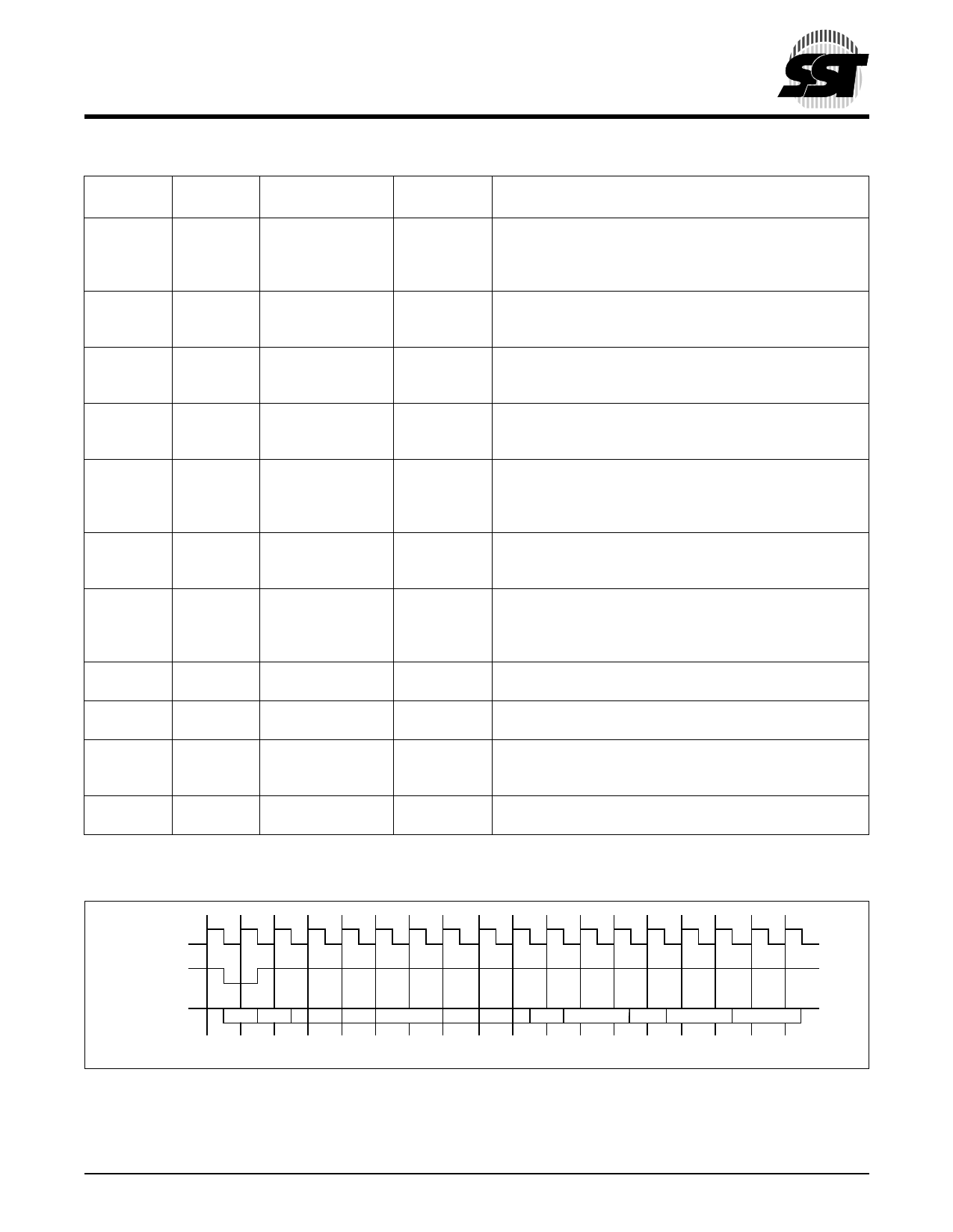
TABLE 1: FWH READ CYCLE
Clock
Cycle
Field
Name
Field Contents
FWH[3:0]1
FWH[3:0]
Direction Comments
1
START
1101
IN
FWH4 must be active (low) for the part to respond. Only the
last start field (before FWH4 transitioning high) should be
recognized. The START field contents indicate a FWH
memory read cycle.
2
IDSEL
0000 to 1111
IN
Indicates which FWH device should respond. If the to IDSEL (ID
select) field matches the value ID[3:0], then that particular device
will respond to the whole bus cycle.
3-9
IMADDR
YYYY
IN
These seven clock cycles make up the 28-bit memory
address. YYYY is one nibble of the entire address.
Addresses are transferred most-significant nibble first.
10
IMSIZE
0000 (1 byte)
IN
A field of this size indicates how many bytes will be or trans-
ferred during multi-byte operations. The SST49LF00xA will
only support single-byte operation. IMSIZE=0000b
11
TAR0
1111
IN
then Float
In this clock cycle, the master (Intel ICH) has driven the bus
then float to all ‘1’s and then floats the bus, prior to the next
clock cycle. This is the first part of the bus “turnaround
cycle.”
12
TAR1
1111 (float)
Float
The SST49LF00xA takes control of the bus during this
then OUT cycle. During the next clock cycle, it will be driving “sync
data.”
13
RSYNC
0000 (READY)
OUT
During this clock cycle, the FWH will generate a “ready-
sync” (RSYNC) indicating that the least-significant nibble of
the least-significant byte will be available during the next
clock cycle.
14
DATA
YYYY
OUT
YYYY is the least-significant nibble of the least-significant
data byte.
15
DATA
YYYY
OUT
YYYY is the most-significant nibble of the least-significant
data byte.
16
TAR0
1111
OUT
then Float
In this clock cycle, the SST49LF00xA has driven the bus to
all ones and then floats the bus prior to the next clock cycle.
This is the first part of the bus “turnaround cycle.”
17
TAR1
1111 (float)
Float then The master (Intel ICH) resumes control of the bus during
IN
this cycle.
1. Field contents are valid on the rising edge of the present clock cycle.
T1.3 504
CLK
FWH4
FWH[3:0]
STR IDS
IMADDR
FIGURE 1: SINGLE-BYTE READ WAVEFORMS
IMS
TAR
RSYNC DATA
TAR
504 ILL F59.1
©2001 Silicon Storage Technology, Inc.
3
S71161-06-000 9/01 504
Share Link: 