ST62E62CD データシートの表示(PDF) - STMicroelectronics
部品番号
コンポーネント説明
メーカー
ST62E62CD
STMicroelectronics

ST62E62CD Datasheet PDF : 72 Pages
| |||
ST62T52CM-Auto ST62T62CM-Auto
MEMORY MAP (Cont’d)
1.3.6 Data RAM/EEPROM
(DRBR)
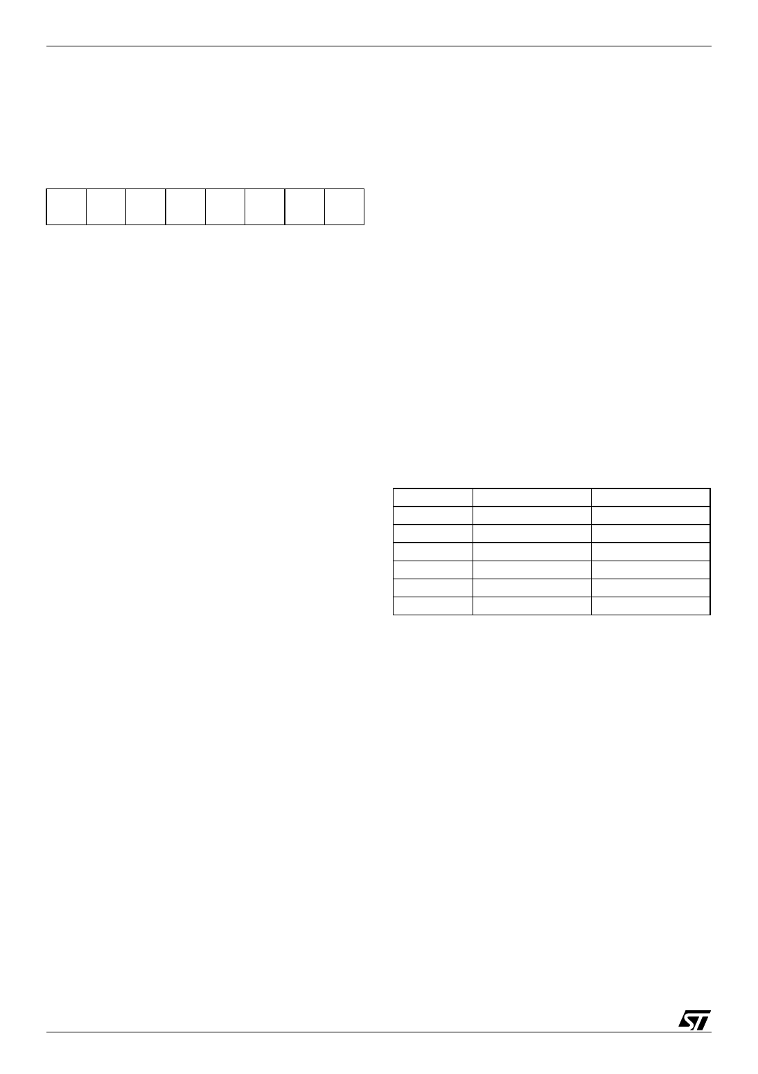
Address: E8h — Write only
Bank
Register
7
0
-
-
-
DRBR
4
-
-
-
DRBR
0
Bit 7-5 = These bits are not used
Bit 4 - DRBR4. This bit, when set, selects RAM
Page 2.
Bit 3-1. Not used
Bit 0. DRBR0. This bit, when set, selects EEP-
ROM page 0.
The selection of the bank is made by programming
the Data RAM Bank Switch register (DRBR regis-
ter) located at address E8h of the Data Space ac-
cording to Table 1. No more than one bank should
be set at a time.
The DRBR register can be addressed like a RAM
Data Space at the address E8h; nevertheless it is
a write only register that cannot be accessed with
single-bit operations. This register is used to select
the desired 64-byte RAM bank of the Data Space.
The bank number has to be loaded in the DRBR
register and the instruction has to point to the se-
lected location as if it was in bank 0 (from 00h ad-
dress to 3Fh address).
This register is not cleared during the MCU initiali-
zation, therefore it must be written before the first
access to the Data Space bank region. Refer to
the Data Space description for additional informa-
tion. The DRBR register is not modified when an
interrupt or a subroutine occurs.
Notes :
Care is required when handling the DRBR register
as it is write only. For this reason, it is not allowed
to change the DRBR contents while executing in-
terrupt service routine, as the service routine can-
not save and then restore its previous content. If it
is impossible to avoid the writing of this register in
interrupt service routine, an image of this register
must be saved in a RAM location, and each time
the program writes to DRBR it must write also to
the image register. The image register must be
written first, so if an interrupt occurs between the
two instructions the DRBR is not affected.
In DRBR Register, only 1 bit must be set. Other-
wise two or more pages are enabled in parallel,
producing errors.
Care must also be taken not to change the
E²PROM page (when available) when the parallel
writing mode is set for the E²PROM, as defined in
EECTL register.
Table 3. Data RAM Bank Register Set-up
DRBR
00
01
02
08
10h
other
ST62T52C
None
Not available
Not Available
Not available
RAM Page 2
Reserved
ST62T62C
None
EEPROM page 0
Not Available
Not available
RAM Page 2
Reserved
10/72
Share Link: