ST7065C データシートの表示(PDF) - Sitronix Technology Co., Ltd.
部品番号
コンポーネント説明
メーカー
ST7065C Datasheet PDF : 14 Pages
| |||
ST7065C
Functional Description:
Shift Registers and Data I/O
The ST7065C supplies two sets of shift register, which controls the shift direction by
SHL1 & SHL2. The DL1, DR1, DL2 and DR2 are data input or output option
function.
Shift Direction of Channel 1
SHL1 Shift Direction DL1 DR1
0
S[1] S[20]
IN OUT
1
S[20] S[1] OUT IN
Shift Direction of Channel 2
SHL2 Shift Direction DL2 DR2
0
S[21] S[40] IN OUT
1
S[40] S[21] OUT IN
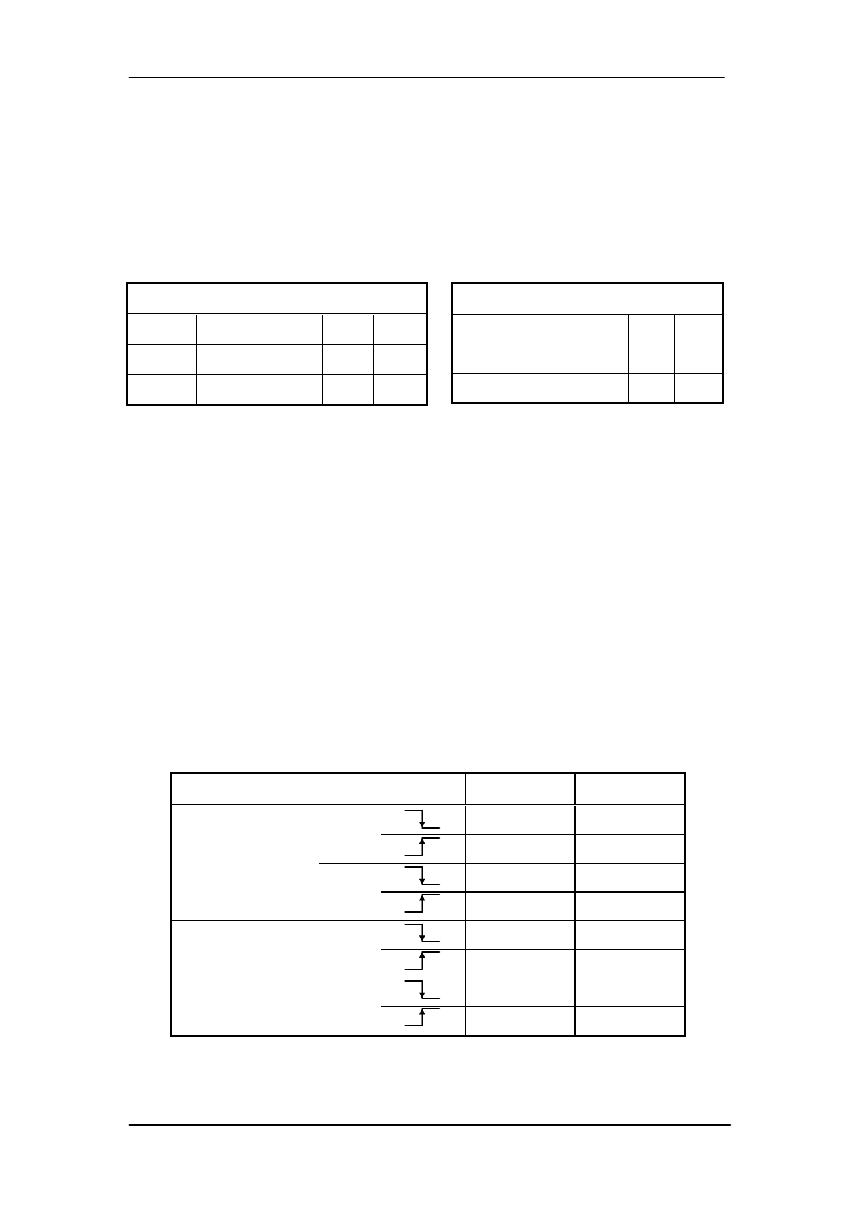
Clock and Mode Selection
In channel 1 part, the CL1 is the clock to latch data on the falling edge. It latches the
data input from the bi-directional shift register at the falling edge of CL1 and transfers
its outputs to the LCD driver circuit. The CL2 is the clock to shift data on the falling
edge. It shifts the serial data at the falling of CL2 and transfers the output of each bit
of the register to the latch circuit.
In channel 2 part, the CL1 and CL2 is the clock to latch or shift data on the falling or
rising edge which is depend on FCS value. When FCS is low, the channel 2 function
is the same as channel 1 as a segment driver. When FCS is high, the channel 2
function will become a common driver. Detail functions are show in the following
table:
FCS
Clock Eage Channel 1 Channel 2
CL1
0
CL2
CL1
1
CL2
Latch data
----
Shift data
----
Latch data
----
Shift data
----
Latch Data
----
Shift data
----
----
Shift data
----
Latch data
V1.4c
8/14
2009/08/21
Share Link: 