ST7541-G データシートの表示(PDF) - Sitronix Technology Co., Ltd.
部品番号
コンポーネント説明
メーカー
ST7541-G Datasheet PDF : 78 Pages
| |||
ST7541
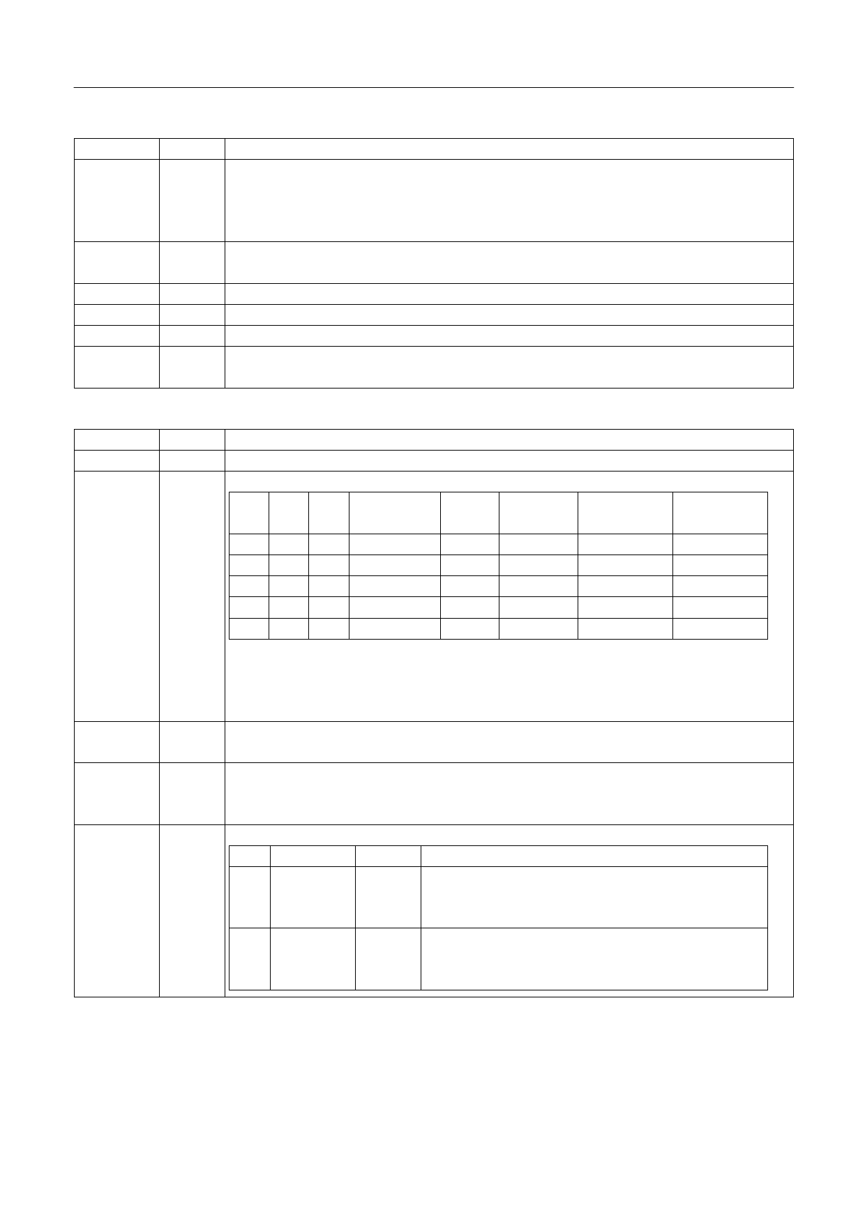
SYSTEM CONTROL
Name
Type
INTRS
I
T[0] ~ T[9] Test
Reserve
X
MF[2:0]
I
DS[1:0]
I
TA, TB
I
Description
Internal resistor select pin. This pin selects the resistors for adjusting V0 voltage level.
INTRS = "H": use the internal resistors.
INTRS = "L": use the external resistors.
VR pin and external resistive divider control V0 voltage
Test pins. Don’ t use these pins.
Please Open these pins.
This pin must be OPEN
Manufacturer ID code for reference, suggest set to [ MF2.MF1.MF0 = 0.0.0 ]
Display size ID code for reference, suggest set to [ DS1.DS0 = 0.0 ]
Test pins
TA and TB must connect to Vss.
MICROPROCESSOR INTERFACE
Name
RST
Type
Description
I
Reset input pin. When RST is “L”, initialization is executed.
Microprocessor interface select input pin
Interface
PS2 PS1 PS0
A0
mode
Data
Read/Write Serial clock
L L H Parallel 80
A0
DB[7:0]
/RD, /WR
-
L H H Parallel 68
A0
DB[7:0]
E, R/W
-
L L L 3Line Serial
-
SID (DB7) Write only SCLK (DB6)
PS[2:0]
I
L H L 4Line Serial A0 SID (DB7) Write only SCLK (DB6)
HL L
IIC Serial
-
SDA
Read/Write
SCL
NOTE:
*1. Reading of data or status is not available in serial interface modes (4-Line, 3-Line and IIC).
*2. In 3-Line or 4-Line interface: DB[5:0], E_RD and RW_WR must be fixed to “H” or “L”.
*3. In IIC and 3-Line interface: A0 must be fixed to “H” or “L”.
CSB
Chip select input. Data/instruction I/O is enabled only when CSB is "L".
I
When chip select is non-active, DB[7:0] will be high impedance.
Register selection input.
A0
I
A0 = "H": DB[7:0] are display data.
A0 = "L": DB[7:0] are control instruction.
Read / Write execution control pin
PS1 MPU type RW_WR
Description
RW_WR
I
H 6800-series
Read / Write control input pin.
R/W R/W = “H” : read;
R/W = “L” : write.
Write enable clock input pin.
L 8080-series /WR The data on DB[7:0] are latched at the rising edge of the
/WR signal.
Ver 1.9
11/78
2007/9/3
Share Link: 