STG3684QTR データシートの表示(PDF) - STMicroelectronics
部品番号
コンポーネント説明
メーカー
STG3684QTR Datasheet PDF : 11 Pages
| |||
STG3684
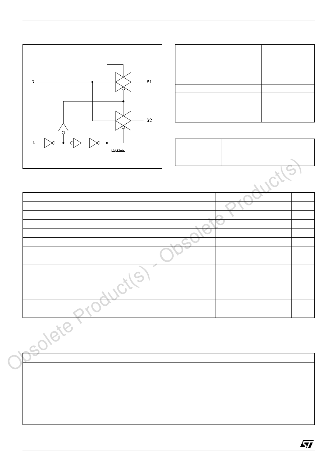
Figure 2: Input Equivalent Circuit
Table 2: Pin Description
QFN
PIN N°
1, 9
2, 10
4, 12
3, 11
5,7,8,13,15,16
6
14
SYMBOL
1IN, 2IN
1S1 to 2S1
1S2 to 2S2
D1, D2
NC
GND
VCC
Table 3: Truth Table
NAME AND
FUNCTION
Controls
Independent Chan-
nels
Common Channels
Not Connected
Ground (0V)
Positive Supply
Voltage
IN
SWITCH S1
SWITCH S2
H
ON
OFF(*)
t(s) Table 4: Absolute Maximum Ratings
L
OFF(*)
ON
(*) High Impedance
duc Symbol
Parameter
ro VCC Supply Voltage
P VI
DC Input Voltage
te VIC
DC Control Input Voltage
le VO
DC Output Voltage
o IIKC
DC Input Diode Current on control pin (VIN < 0V)
s IIK
DC Input Diode Current (VIN < 0V)
b IOK
DC Output Diode Current
- O IO
DC Output Current
) IOP
DC Output Current Peak (pulse at 1ms, 10% duty cycle)
t(s ICC or IGND DC VCC or Ground Current
c PD
Power Dissipation at Ta=70°C (1)
du Tstg
Storage Temperature
ro TL
Lead Temperature (10 sec)
Value
-0.5 to 4.6
-0.5 to VCC + 0.5
-0.5 to 4.6
-0.5 to VCC + 0.5
− 50
± 50
± 20
± 300
± 500
± 100
1120
-65 to 150
300
Unit
V
V
V
V
mA
mA
mA
mA
mA
mA
mW
°C
°C
P Absolute Maximum Ratings are those values beyond which damage to the device may occur. Functional operation under these conditions is
not implied.
te (1) Derate above 70°C: by 18.5mW/°C.
le Table 5: Recommended Operating Conditions
so Symbol
Parameter
ObVCC Supply Voltage (note 1)
Value
Unit
1.65 to 4.3
V
VI
Input Voltage
0 to VCC
V
VIC Control Input Voltage
0 to 4.3
V
VO
Output Voltage
0 to VCC
V
Top
Operating Temperature
-55 to 125
°C
Input Rise and Fall Time Control Input
dt/dv
VCC= 1.65V to 2.7V
VCC= 3.0V to 4.3V
0 to 20
0 to 10
ns/V
1) Truth Table guaranteed: 1.2V to 4.3V.
2/11
Share Link: 