STG3690 データシートの表示(PDF) - STMicroelectronics
部品番号
コンポーネント説明
メーカー
STG3690 Datasheet PDF : 12 Pages
| |||
STG3690
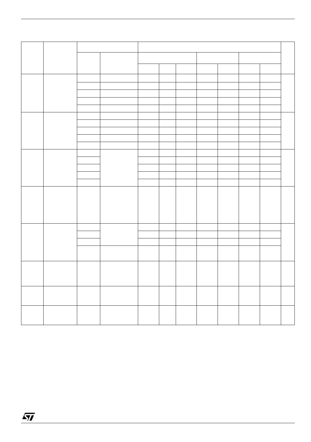
Table 5: DC Specifications
Test Conditions
Value
Symbol Parameter VCC
(V)
TA = 25°C
Min. Typ. Max.
-40 to 85°C
Min. Max.
-55 to 125°C Unit
Min. Max.
VIH High Level 1.65-1.95
Input Voltage 2.3-2.5
0.65VCC
1.4
0.65VCC
1.4
0.65VCC
1.4
2.7-3.0
1.4
1.4
1.4
V
3.3
1.5
1.5
1.5
3.6
1.7
1.7
1.7
VIL Low Level 1.65-1.95
Input Voltage 2.3-2.5
0.40
0.40
0.40
0.50
0.50
0.50
2.7-3.6
0.50
0.50
0.50 V
3.3
0.50
0.50
0.50
3.6
0.50
0.50
0.50
RON Switch ON
3.0
1.15 1.5
1.8
Resistance
(1)
2.7
2.3
1.8
VS=0V to VCC
IS=100mA
1.30 1.7
1.45 2.0
1.70 3.2
2.0
2.4
3.7
Ω
1.65
1.80 3.5
4.0
∆RON ON
Resistance
Match
between
2.7
VS=1.5V
IS=100mA
0.06
Ω
channels
(1,2)
RFLAT ON
3.0
Resistance
2.7
FLATNESS
(3)
2.3
VS=1.5V
IS=100mA
0.07 0.15
0.15
Ω
1.65
VS=0.8V
IS=100mA
IOFF OFF State
3.3 VS=0.3 or 3V
±10
± 100
nA
Leakage
Current
(nSn), (Dn)
IIN Input
0 - 3.6 VIN= 0 to 3.6V
±0.1
±1
µA
Leakage
Current
ICC Quiescent 1.65-3.6 VIN=VCC or
Supply
GND
Current (1)
±0.05
±0.2
±1 µA
Note 1: Guaranteed by design
Note 2: ∆RON = RON(MAX) - RON(MIN).
Note 3: Flatness is defined as the difference between the maximum and minimum value of on-resistance as measured over the specified
analog signal ranges.
3/12
Share Link: 