STG3693 データシートの表示(PDF) - STMicroelectronics
部品番号
コンポーネント説明
メーカー
STG3693 Datasheet PDF : 19 Pages
| |||
STG3693
Electrical characteristics
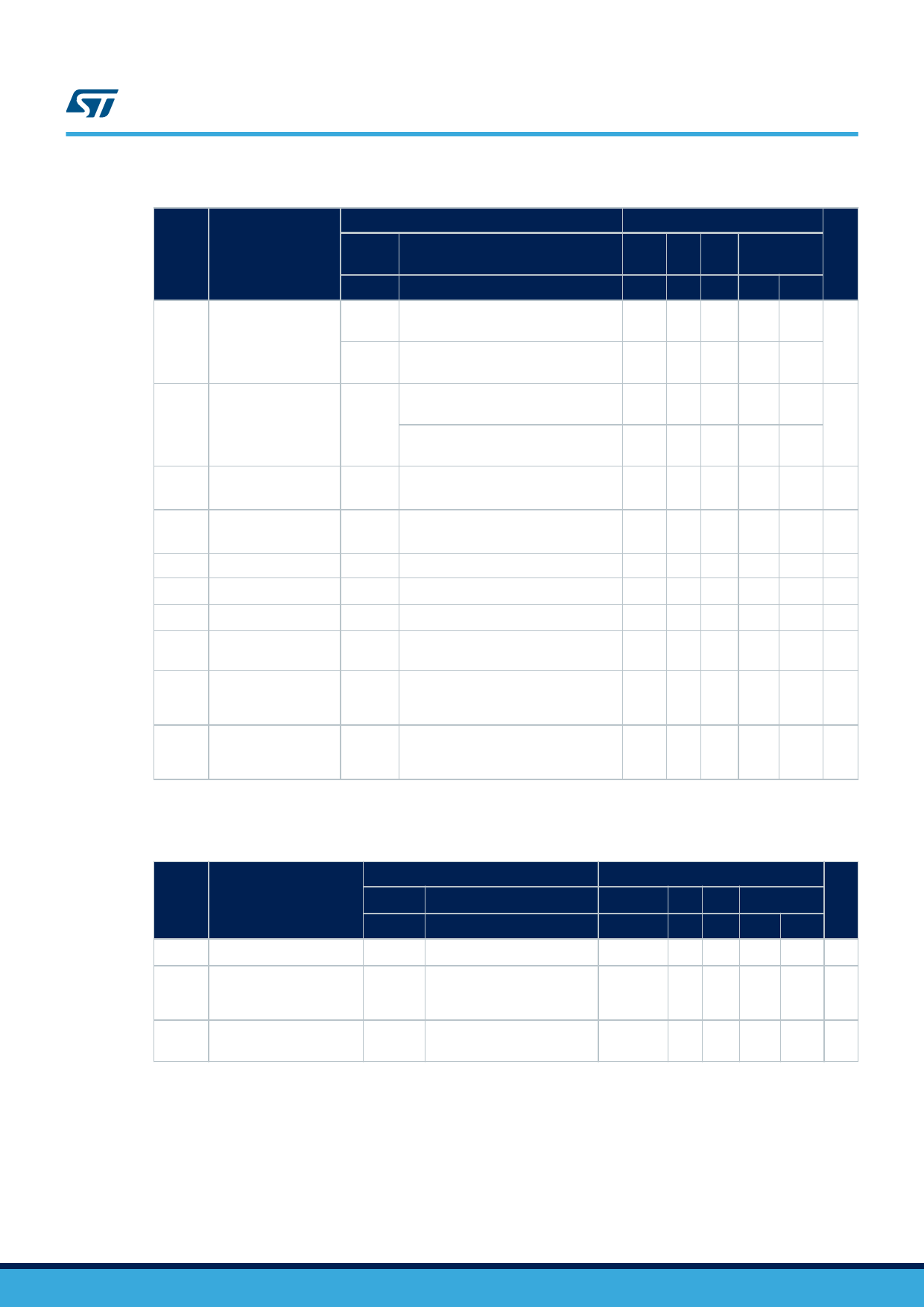
Table 7. Analog switch characteristics (CL = 5 pF, RL = 50 Ω, TA = 25 °C)
Test conditions
Value
Symbol
Parameter
VCC (V)
TA =
25 °C
-40 to 125 °C Unit
Min. Typ. Max. Min. Max.
1.65 -4.3
VS = 1 VRMS, f =1 MHz, signal = 0
dBm
-79
OIRR
Off isolation(1)
dB
VS = 1 VRMS, f =1 MHz, signal = 0
dBm
-60
VS = 1 VRMS, f =1 MHz, signal = 0
dBm
-78
Xtalk
Crosstalk
1.65 -4.3
dB
VS = 1 VRMS, f =1 MHz, signal = 0
dBm
-61
THD
Total harmonic
distortion
3.7
f = 20 Hz to 20 kHz, RL = 32 Ω, CL=50
Ω, VIN = 2.8 VP-P, VDC = VCC/2
0.01 0.02
%
PSRR
Power supply
rejection ratio
3.7
f = 217 Hz, RL = 32 Ω, CL=50 Ω,
Vripple = 150 mV, VDC = VCC/2
-60
dB
BW
-3 dB bandwidth
3.0-4.3
RL = 50 Ω, signal= 0 dBm
800
MHz
DG
Differential gain
3.0-4.3
RL = 150 Ω
0.64
%
DP
Differential phase 3.0-4.3
RL = 150 Ω
0.1
deg
CIN
Control pin input
capacitance
VCC = 0 V
6.2
pF
Sn port capacitance
CON
when switch is
3.3
f = 1 MHz
10
pF
enabled
Sn port capacitance
COFF
when switch is
3.3
f = 1 MHz
5
pF
disabled
1. Off Isolation = 20 Log10 (VD/VS), VD = output. VS = input to off switch.
Table 8. USB related AC electrical characteristics
Test conditions
Value
Symbol
Parameter
VCC (V)
TA = 25 °C
-40 to 125 °C Unit
Min. Typ. Max. Min. Max.
tSK(0) Channel-to-channel skew 3.0 to 3.6 CL=10 pF
26
ps
Skew of opposite
tSK(P)
transition of the same 3.0 to 3.6
CL=10 pF
60
ps
output
TJ
Total jitter
3.0 to 3.6
RL = 50 Ω, CL= 10 pF, tR = tF
= 750 ps at 480 Mbps
130
dB
DS5044 - Rev 5
page 7/19
Share Link: 