STK621-031 データシートの表示(PDF) - SANYO -> Panasonic
部品番号
コンポーネント説明
メーカー
STK621-031 Datasheet PDF : 10 Pages
| |||
STK621‑031
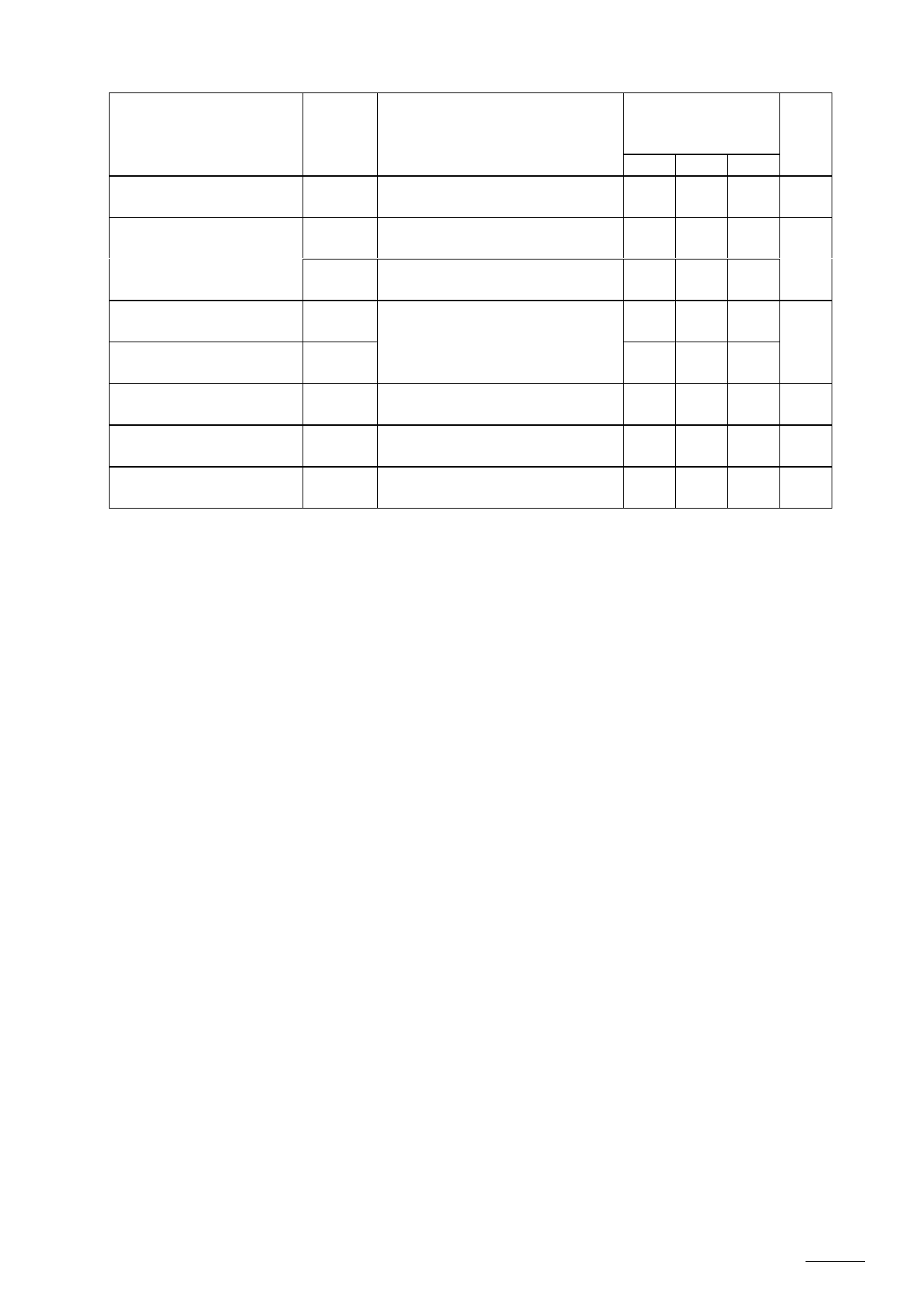
推奨動作条件/The Recommendation Operating Conditions
推奨使用条件
項目
Parameters
記号
Symbol
条
件
Conditions
The Recommendation 単位
Operating Conditions Unit
Min. Typ. Max.
電源電圧
Supply voltage
+ ‑ −端子
VCC
+‑−
0 280 400 V
制御電源電圧
VD1,2,3
Pre‑driver supply voltage
VD4
VB1 ‑ U,VB2 ‑ V,VB3 ‑ W 間
VB1 ‑ U,VB2 ‑ V,VB3 ‑ W
VDD ‑ VSS 間
VDD ‑ VSS ※1
12.5 15 17.5
V
13.5 15 16.5
ON 入力信号電圧
Input ON voltage
OFF 入力信号電圧
Input OFF voltage
HIN1,HIN2,HIN3,
VIN(ON) LIN1,LIN2,LIN3 端子間
HIN1,HIN2,HIN3,
VIN(OFF) LIN1,LIN2,LIN3 Terminal
0
−
1
V
4
5 VDD
PWM周波数
PWM frequency
fPWM
1
− 10 KHZ
デッドタイム
Deadtime
上下相入力信号休止時間
DT
Upper/lower input signal downtime 2
− − μs
締め付けトルク
Tightening torque
取り付けネジM4
MT
M4 Type Screw
0.79 − 1.17 N・m
※1.制御電源 VD4=15±1.5V は、IO=20mA(DC),0.5A(Peak)の容量があること。
Pre‑driver power supply (VD4=15±1.5V) must have the capacity of IO=20mA(DC), 0.5A(Peak).
注意事項/Usage Precautions
1.ブートストラップ用ダイオード:DB(耐圧 600V 以上で trr の短い高速ダイオードを使用して下さい)及びコンデン
サ CB(1〜47μF 程度)を取り付けることにより制御電源を1電源で駆動できます。この場合、下側素子を ON (出力
を LOW)にして CB を充電させます。尚、起動時等、CB の電圧が低いときは大きな充電電流が流れ、ノイズ等の悪影響
を及ぼす原因となる場合があります。制限抵抗 RB(数Ω〜数十Ω程度)を取り付けて下さい。
(ブートストラップ法を用いない場合は上側各制御電源に独立した電源を外部供給して下さい。)
また、制御方法によっては上側電源電圧が不足する場合があります。確認して下さい。
By the addition of the diode for the bootstrap (DB : high speed type, withstand voltage equal to or more
than 600V) and of the capacitor (CB : about 1 to 47μF), a single power supply drive is enabled. In
this case, it makes a lower side IGBT ON (input signal of lower side makes LOW). Then it charges in CB.
Incidentally, in case of start‑up and so on, when the voltage of CB is low, the big charging electric
current flows and sometimes becomes the cause which exerts the bad influence of the noise and so on.
Put limitation resistance RB (Several Ω to about tens of Ω). (When not using bootstrap circuit, each
upper side pre‑drive power supply needs an independent power supply. Externally set.) Also, the upper
side power supply voltage sometimes declines by the way of controlling. Confirm it.
2.+、−端子電源外部配線の浮遊インダクタンス等の影響でスイッチング動作時に振動を伴う跳ね上がり電圧が発
生しますので、配線長(CI から各端子間)を短くして配線インダクタンスを小さくすると伴に、+と−端子間ので
きるだけ近くに電圧吸収用スナバ回路(コンデンサ/CS/0.1〜10μF 程度)を接続するなどしてサージ電圧を抑制し
て下さい。
Because the jump voltage which is accompanied by the vibration in case of switching operation occurs
by the influence of the floating inductance of the wiring of the outer power supply which is connected
with of the + terminal and the – terminal, restrains and spares serge voltage being as the connection
of the snubber circuit (Capacitor / CS / about 0.1 ‑ 10 μF) for the voltage absorption with the neighborhood
as possible between + and the ‑ terminal, and so on, with making a wiring length (among the terminals
each from CI) short and making a wiring inductance small.
(−
)
No. 8
Share Link: 