STK621-041 データシートの表示(PDF) - SANYO -> Panasonic
部品番号
コンポーネント説明
メーカー
STK621-041
SANYO -> Panasonic

STK621-041 Datasheet PDF : 13 Pages
| |||
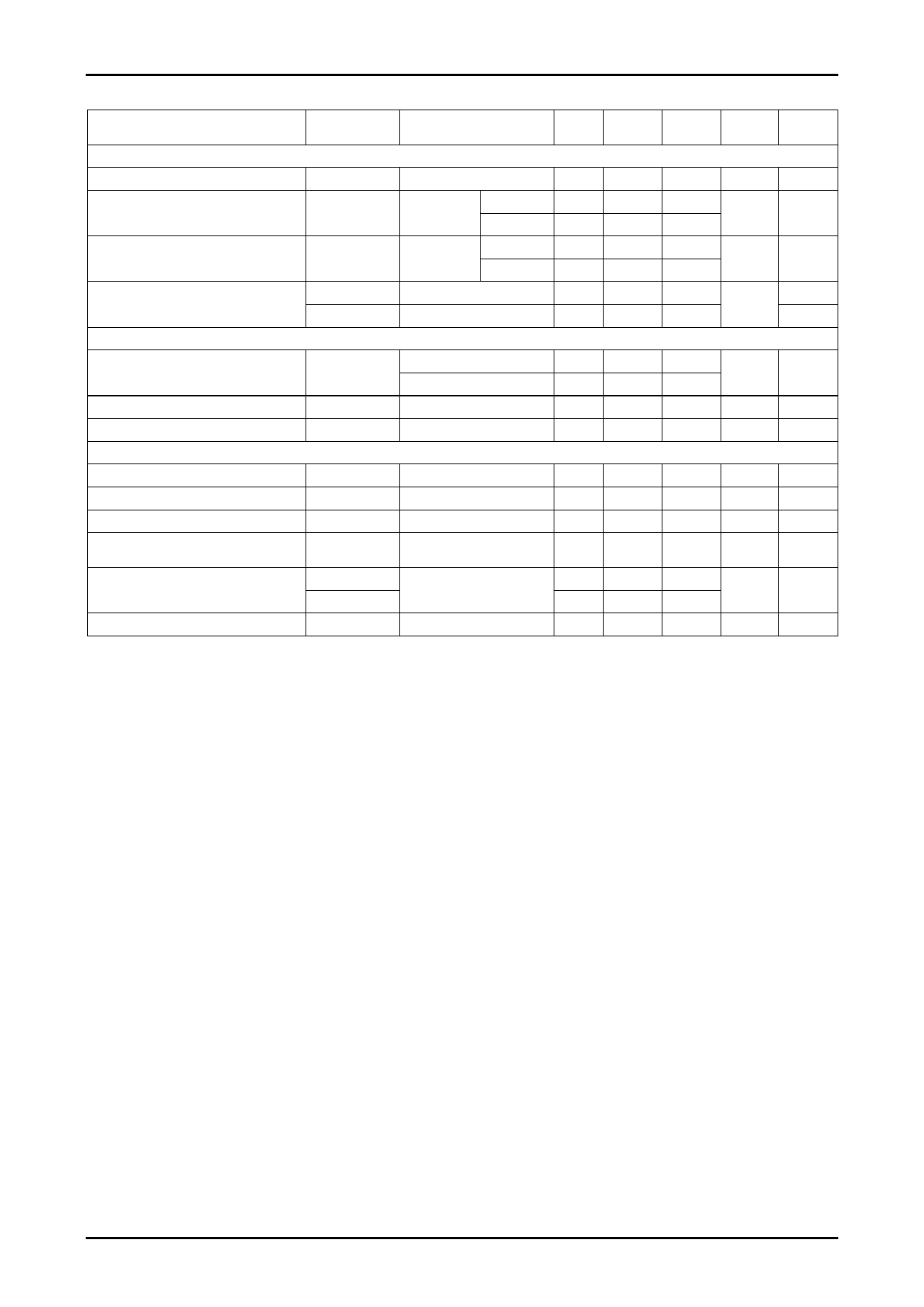
STK621-041,621-041A-E
Electrical Characteristics at Tc=25°C, VD=15V
Parameters
Symbols
Conditions
min
Power output block
Collector-to-emitter cut-off current
Collector-to-emitter saturation voltage
ICE
VCE(SAT)
VCE=600V
IO=10A
Upper side
Lower side
Diode forward voltage
VF
IO=-10A
Upper side
Lower side
Junction-to-substrate thermal resistance Rthj-c(T)
IGBT
Rthj-c(D)
FWD
Control (Pre-driver) block
Control circuit current dissipation
ID
VD1, 2, 3=15V
VD4=15V
ON input signal voltage
VIH
Output ON
OFF input signal voltage
VIL
Output OFF
2.2
Protection block
Thermal protection temperature
TSD
Substrate surface
100
Overcurrent protection current
ISD
P.W.=100µs
28
Control supply under voltage protection
UVLO
9
FAULT pin intake current
Switching time
IOSD
TON
When FAULT operating
(Low), VFAULT=1V
IO=10A, Inductive load
TOFF
Current output signal level
ISO
IO=10A
Unless otherwise specified, the voltage reference for - pins is the VSS pin voltage.
typ
1.6
1.8
1.7
1.9
3.0
3.6
0.05
10
2
1.0
1.2
0.167
max
unit
2.0
mA
2.2
V
2.4
2.3
V
2.5
°C/W
mA
0.8
V
V
120
°C
40
A
12
V
mA
µs
V
Test
circuit
Fig.1
Fig.2
Fig.3
Fig.4
Fig.5
Fig.6
Notes
1. The ON input signal voltage prescribes the input signal voltage at which the output stage IGBT turns ON, and the
OFF input signal voltage prescribes the input signal voltage at which the output stage IGBT turns OFF.
Apply a voltage between 0 and VIH (max) when output is ON, and a voltage between VIL (min) and VDD when
output is OFF.
2. After the internal protection circuit operates and the FAULT signal (Low = FAULT ON: open drain output) goes
ON, the latch status continues as long as any of the six input signals is ON (Low). The latch status is reset after all
six input signals are OFF (High) continuously for approximately 10µs.
However, control supply under voltage protection (UVLO) operation is as follows.
Upper arm → The FAULT signal is not output, but the corresponding gate signal turns OFF.
Note that even if the voltage recovers to normal, the latch status continues while the input signal
is ON (Low).
Lower arm → The gate signal goes OFF and FAULT signal is output.
However, unlike protection operation for the upper arm, operation returns to normal when the
voltage recovers to normal. (Protection operation is not latched by the input signal.)
3. When using M4 screws to mount the IC to a heat sink plate, apply a tightening torque of 0.79 to 1.17 N•m. The
heat sink plate-mounting flatness should be 0.25mm or less.
4. The control supply voltage-drop protection function protects the devices when the control supply voltage drops due
to some abnormality during operation. Control supply voltage drop at the start of operation and other cases should
be confirmed in the set-mounted condition.
No. A0483-3/13
Share Link: