STK621-041A-E データシートの表示(PDF) - SANYO -> Panasonic
部品番号
コンポーネント説明
メーカー
STK621-041A-E
SANYO -> Panasonic

STK621-041A-E Datasheet PDF : 13 Pages
| |||
STK621-041,621-041A-E
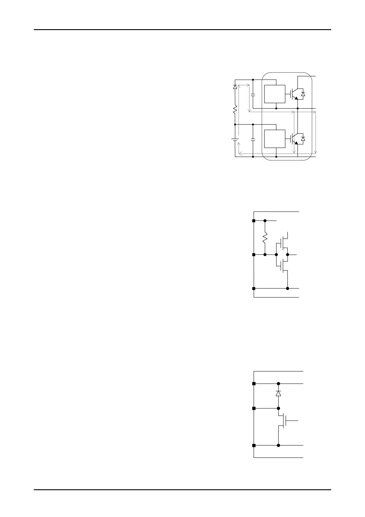
(4) VB1, VB2 and VB3 pins
These pins connect the positive power supplies for the upper-side
power device pre-driver circuits. The three control power supplies
each require an electrically insulated floating power supply. In
addition to the method that uses three independent power supplies,
STK621-041,041A-E
this power supply can also be configured using the bootstrap circuit
shown in Fig. 3. As shown in this figure, CB has a path (1) that is
DB
charged when the lower-side device is ON, and a path (2) for motor
regeneration mode. The CB section voltage fluctuates according to the
CB
Driver
switching frequency and duty ratio of the external control circuit.
Therefore, the CB capacitance value must be set in consideration of
the voltage fluctuation. DB should use a high-speed type FRD with a
(1)
(2)
fast trr and VR = 600V. RB is used to limit the rush charging current
during CB initial charging. Note that a large rush charging current VDD
may cause the internal circuits to malfunction. CB can also be charged
Driver
before startup by connecting high-value resistors to the output pins
and minus pins. (Care must be taken for the withstand voltage and the
power.)
The upper-side control power supply voltage is monitored by the
Figure 3 Bootstrap circuit and charge path
under voltage protection circuit, and the respective phase output stops
when the voltage is insufficient.)
(5) Input (HIN1, HIN2, HIN3, LIN1, LIN2, LIN3) pins
Fig. 4 shows the input pin internal circuit. In the input block, the VDD
pin is pulled up internally by a 50kΩ resistor. The input signal is low
active, and output is ON at a voltage of VIH (max) or less, and OFF at
a voltage of VIL (min) or more. This allows direct input to the input
pin from a 5V control circuit. When using direct connection from the
control circuit, the connection block on the control circuit side is
pulled up by a 50kΩ resistor, so the voltage potential may be higher
than 5V. In cases when this voltage may exceed the withstand voltage
of the connection block, an effective measure is to connect an external
resistor of several kΩ between the external 5V power supply and the
input pin. Note that this external resistor also effectively absorbs input
pin noise when the pin is susceptible to noise in an actual set. HIN1,
HIN2 and HIN3 are the inputs for the U, V and W upper-side power
devices, and LIN1, LIN2 and LIN3 are the inputs for the lower-side
power devices. An anti-simultaneous ON circuit is built-in to prevent
arm short-circuits when both the upper and lower inputs for each
phase are ON at the same time. However, a dead time must always be
provided between signals to prevent arm short-circuits due to the
power device switching response delay.
VDD
50kΩ
IN
VSS
Figure 4 Input circuit block
(6) FAULT pin
The FAULT pin is an open drain output as shown in Fig. 5. When
protection operation starts, the MOSFET turns ON and the FAULT
pin goes Low. At this time, the intake current IOSD is 2mA (at
voltage of 1V). This should be taken into account when connecting an
external circuit. When pulling up the pin with a resistor, connect
5.6kΩ or more.
The protection circuits that operate the FAULT pin are the overcurrent
protection circuit and the lower-side drive supply voltage (VDD -
VSS) under-voltage protection circuit. The FAULT pin does not
operate during upper-side power supply under-voltage protection. All
power devices are OFF while the FAULT pin is Low. FAULT is
latched when any of the inputs are ON (except VDUV), and is reset
by turning all six inputs OFF.
VDD
FAULT
VSS
Figure 5 FAULT output block
No. A0483-8/13
Share Link: