STK672-740B-E データシートの表示(PDF) - SANYO -> Panasonic
部品番号
コンポーネント説明
メーカー
STK672-740B-E Datasheet PDF : 23 Pages
| |||
STK672-740B-E
Specifications
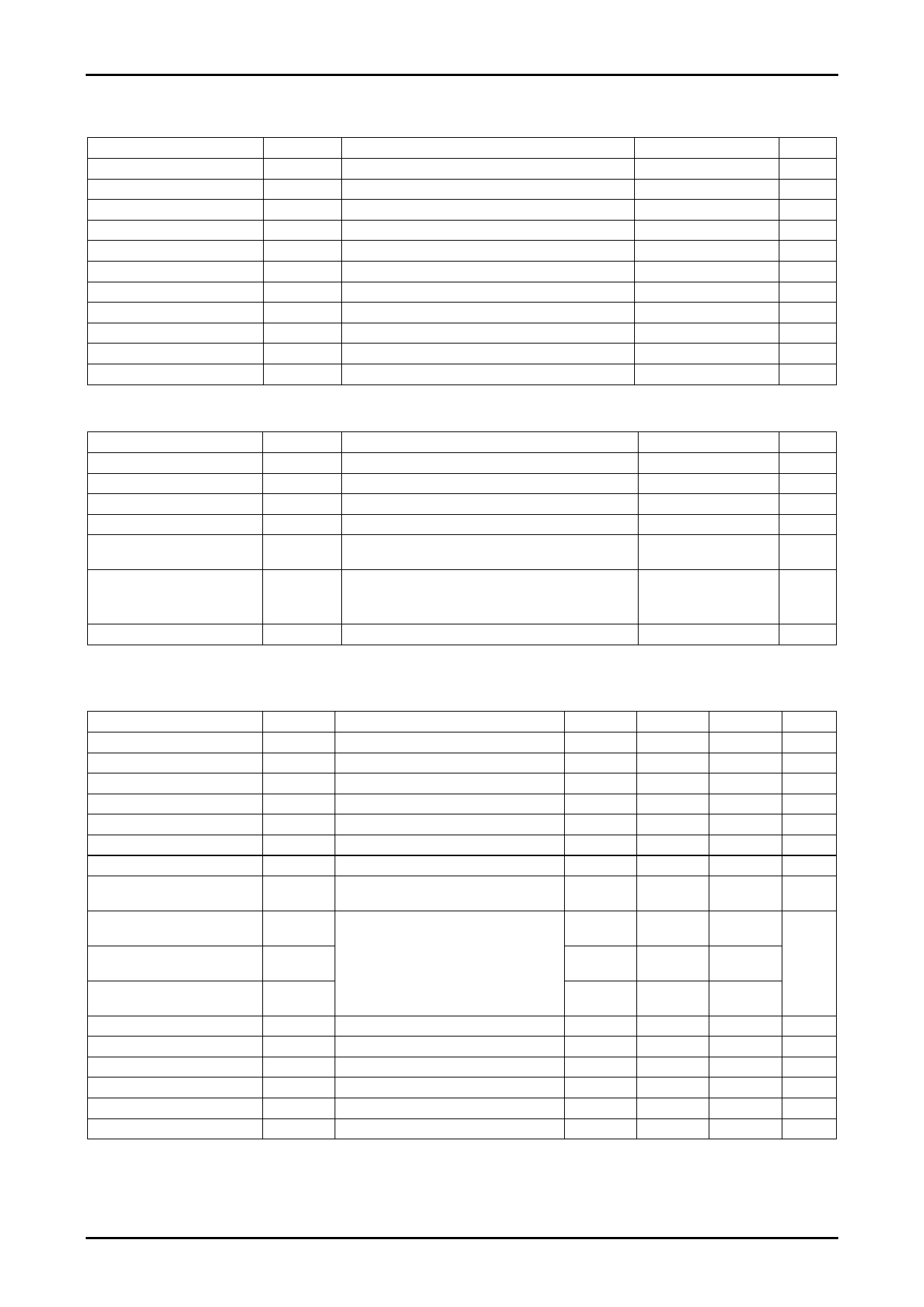
Absolute Maximum Ratings at Tc = 25°C
Parameter
Maximum supply voltage 1
Maximum supply voltage 2
Input voltage
Output current 1
Output current 2
Output current 3
Allowable power dissipation 1
Allowable power dissipation 2
Operating substrate temperature
Junction temperature
Storage temperature
Symbol
VCC max
VDD max
VIN max
IOP max
IOH max
IOF max
PdMF max
PdPK max
Tc
Tj max
Tstg
Conditions
No signal
No signal
Logic input pins
10μs, 1 pulse (resistance load)
VDD=5V, CLOCK≥200Hz
Pin16 output current
With an arbitrarily large heat sink. Per MOSFET
No heat sink
Metal surface temperature of the package
Ratings
unit
50
V
-0.3 to +6.0
V
-0.3 to +6.0
V
20
A
4
A
10
mA
8.3
W
3.1
W
-20 to +105
°C
150
°C
-40 to +125
°C
Allowable Operating Ranges at Ta=25°C
Parameter
Symbol
Conditions
Operating supply voltage 1
VCC
With signals applied
Operating supply voltage 2
VDD
With signals applied
Input high voltage
VIH
Pins 13, 17, 12, 10, 14, 15
Input low voltage
Output current 1
VIL
IOH1
Pins 13, 17, 12, 10, 14, 15
Tc=105°C, CLOCK≥200Hz,
Continuous operation, duty=100%
Output current 2
Recommended Vref range
IOH2
Vref
Tc=80°C, CLOCK≥200Hz,
Continuous operation, duty=100%,
See the motor current (IOH) derating curve
(* CLOCK ≥ 200Hz is the same as 200pps or more.)
Ratings
unit
0 to 46
V
5±5%
V
2.5 to VDD
V
0 to 0.8
V
3.0
A
3.3
A
0.14 to 1.31
V
Electrical Characteristics at Tc=25°C, VCC=24V, VDD=5.0V
Parameter
Symbol
Conditions
min
typ
max
unit
VDD supply current
Output average current
ICCO
Ioave
Pin 9 current
R/L=1Ω/0.62mH in each phase
0.519
5
0.625
8
mA
0.731
A
FET diode forward voltage
Output saturation voltage
Input high voltage
Input low voltage
FAULT1 low output voltage
5V level FAULT1 leakage
current
Vdf
Vsat
VIH
VIL
VOLF
IILF
If=1A (RL=23Ω)
RL=23Ω
Pins 13, 17, 12, 10, 14, 15
Pins 13, 17, 12, 10, 14, 15
Pin 16 (IO=5mA)
Pin 16=5V
0.83
1.5
V
0.20
0.33
V
2.5
V
0.8
V
0.25
0.5
V
10
μA
FAULT2 Motor terminal open
detection output voltage
VOF1
Pin 8 (when all protection functions have
been activated)
0.00
0.01
0.20
FAULT2 Overcurrent detection
output voltage
VOF2
2.4
2.5
2.6
V
FAULT2 Overheat detection
output voltage
5V level input current
GND level input current
Vref input bias current
PWM frequency
VOF3
IILH
IILL
IIB
fc
Pins 13, 17, 12, 10, 14, 15=5V
Pins 13, 17, 12, 10, 14, 15=GND
Pin 19=1.0V
3.1
3.3
3.5
50
75
μA
10
μA
1
μA
29
45
61 kHz
Overheat detection temperature TSD
Design guarantee
144
°C
Drain-source cut-off current
IDSS
VDS=100V, Pins 2, 6, 9, 18=GND
1
μA
* Operation at the maximum VCC value may not be possible, depending on the motor current. See “8. Other Notes on
Use” in the Data Sheet for details.
*Ioave values are for when the lead frame of the product is soldered to the mounting substrate.
Notes: A fixed-voltage power supply must be used.
No. A1932-2/23
Share Link: 