T431616D データシートの表示(PDF) - Taiwan Memory Technology
部品番号
コンポーネント説明
メーカー
T431616D Datasheet PDF : 74 Pages
| |||
tm TE
CH
CLK
DQM
T0
T1
T2
T3
T4
T5
1 Clk Interval
T431616D/E
T6
T7
T8
COMMAND
NOP
NOP
BANKA
ACTIVATE
NOP
READ A WRITE A
NOP
NOP
CAS# latency=1
tCK1, DQ's
CAS# latency=2
tCK2, DQ's
: "H" or "L"
Must be Hi-Z before
the Write Command
DIN A0
DIN A0
DIN A1
DIN A1
DIN A2
DIN A2
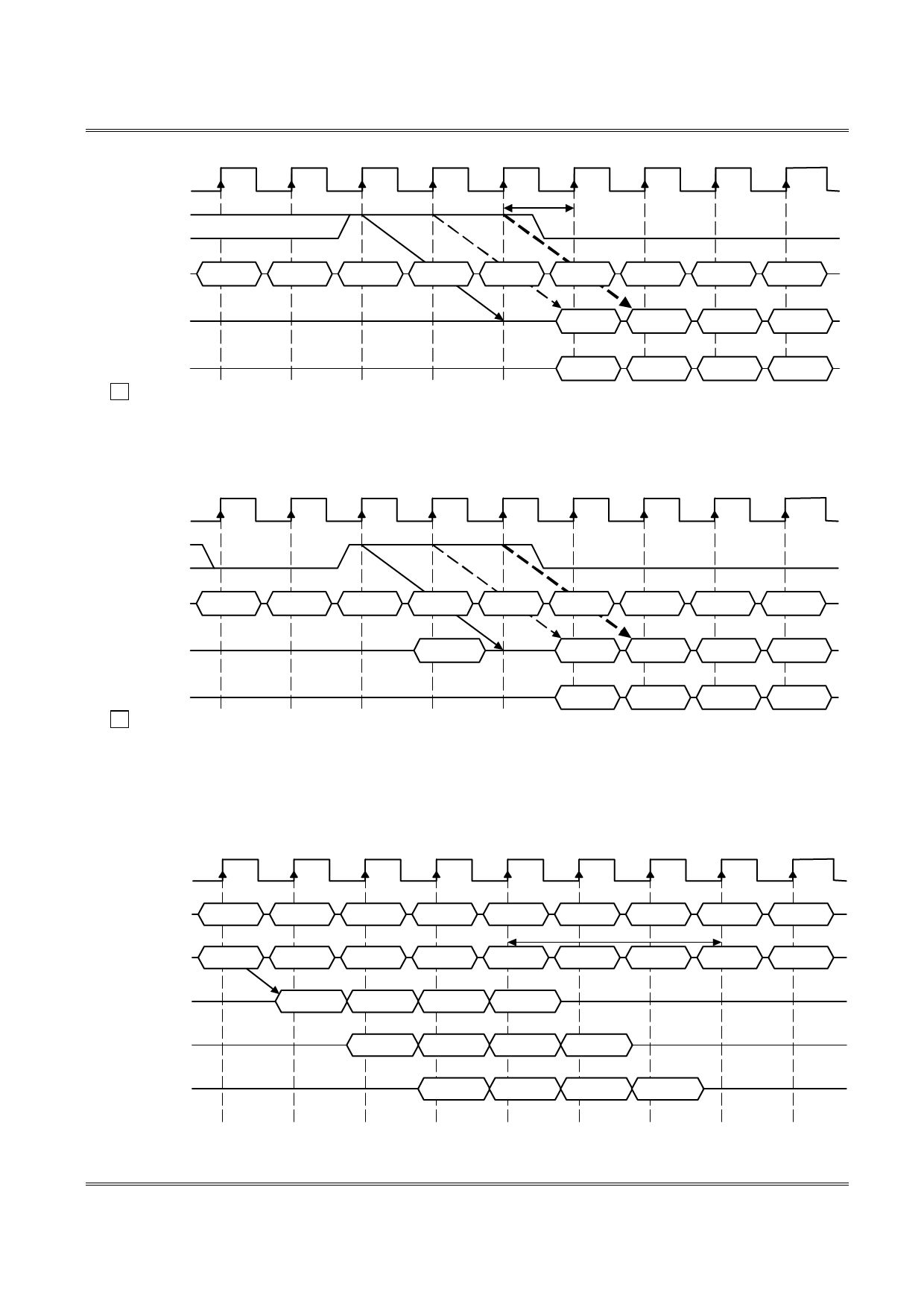
Read to Write Interval (Burst Length ≥ 4, CAS# Latency = 1, 2)
NOP
DIN A3
DIN A3
CLK
DQM
T0
T1
T2
T3
T4
T5
T6
T7
T8
COMMAND
NOP
NOP
READ A
NOP
NOP
WRITE B
NOP
NOP
NOP
CAS# latency=1
tCK1, DQ's
CAS# latency=2
tCK2, DQ's
: "H" or "L"
DOUT A0
DIN B0
Must be Hi-Z before
the Write Command
DIN B0
DIN B1
DIN B1
DIN B2
DIN B3
DIN B2
DIN B3
Read to Write Interval (Burst Length ≥ 4, CAS# Latency = 1, 2)
A read burst without the auto precharge function may be interrupted by a BankPrecharge/ PrechargeAll
command to the same bank. The following figure shows the optimum time that BankPrecharge/ PrechargeAll
command is issued in different CAS# latency.
T0
T1
T2
T3
T4
T5
T6
T7
T8
CL K
ADDR ESS
COMMAND
Bank,
Col A
READ A
NOP
NOP
NOP
Bank (s)
Precharge
tRP
NOP
NOP
Bank,
Row
Activate
NOP
CAS# latency=1
tCK1 , DQ's
CAS# la tency=2
tCK2 , DQ's
CAS# la tency=3
tCK3 , DQ's
DOUT A0
DOUT A1 DOUT A2
DOUT A3
DOUT A0
DOUT A1 DOUT A2
DOUT A3
DOUT A0
DOUT A1 DOUT A2
DOUT A3
Read to Precharge (CAS# Latency = 1, 2, 3)
TM Technology Inc. reserves the right
P. 8
to change products or specifications without notice.
Publication Date: FEB. 2007
Revision: A
Share Link: 