TA8053 データシートの表示(PDF) - Toshiba
部品番号
コンポーネント説明
メーカー
TA8053 Datasheet PDF : 10 Pages
| |||
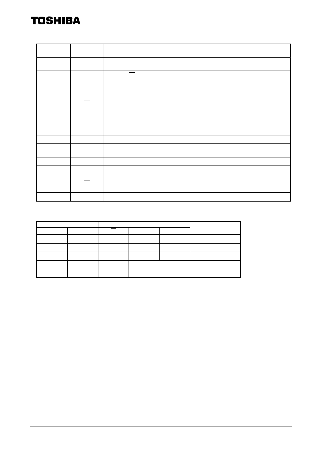
PIN DESCRIPTION
TA8053H
PIN No.
1
2
3
4
5
7
9
10
11
12
6, 8
SYMBOL
DI1
DI2
TD
DG
M (+)
GND
M (-)
VCC
VS
ST
NC
DESCRIPTION
Output status control pin.
Connects to a PNP-type voltage comparator.
Delays the DG output. A capacitor is placed between this pin and GND.When the pin is open,
DG is in switching state.
Self-diagnostic output pin. When the output current increases above 6A (typically), a switching
waveform is output from this pin as from M (+) and M (−). If a capacitor is connected to the TD
pin, the signal from this pin will go low after a certain delay. The output is an open-collector
output.
The delay time is approximately calculated by the following formula :
TD (ms)=50×CT (µF)
Permissible CT range : 0.01µF to 2µF
Connects to the DC motor. Both the sink and the source have a current capacity of 3A. Diodes
for absorbing counter electromotive force are contained on the VCC and GND sides.
Grounded
Connects to the DC motor together with pin 5 and has the same function as pin 5. This pin is
controlled by the inputs from pins 1 and 2.
Power supply pin for the output section
Power supply pin for the control section. This pin is completely separated from the VCC pin.
When this pin is opened or grounded, the output turns off to reduce the current consumption
below 100µA.
If standby mode is not needed, the pin is connected to VCC.
Not connected. (Electrically, this pin is completely open.)
TRUTH TABLE
INPUT
DI1
DI2
H
H
L
H
H
L
L
L
H/L
H/L
OUTPUT
ST
M (+)
M (−)
OUTPUT MODE
H
L
L
BRAKE
H
L
H
REVERSE
H
H
L
FORWARD
H
OFF (high impedance)
STOP
L
OFF (high impedance)
STANDBY
2
2002-01-30
Share Link: 