TA8248 データシートの表示(PDF) - Toshiba
部品番号
コンポーネント説明
メーカー
TA8248 Datasheet PDF : 12 Pages
| |||
Application Information And Application Method
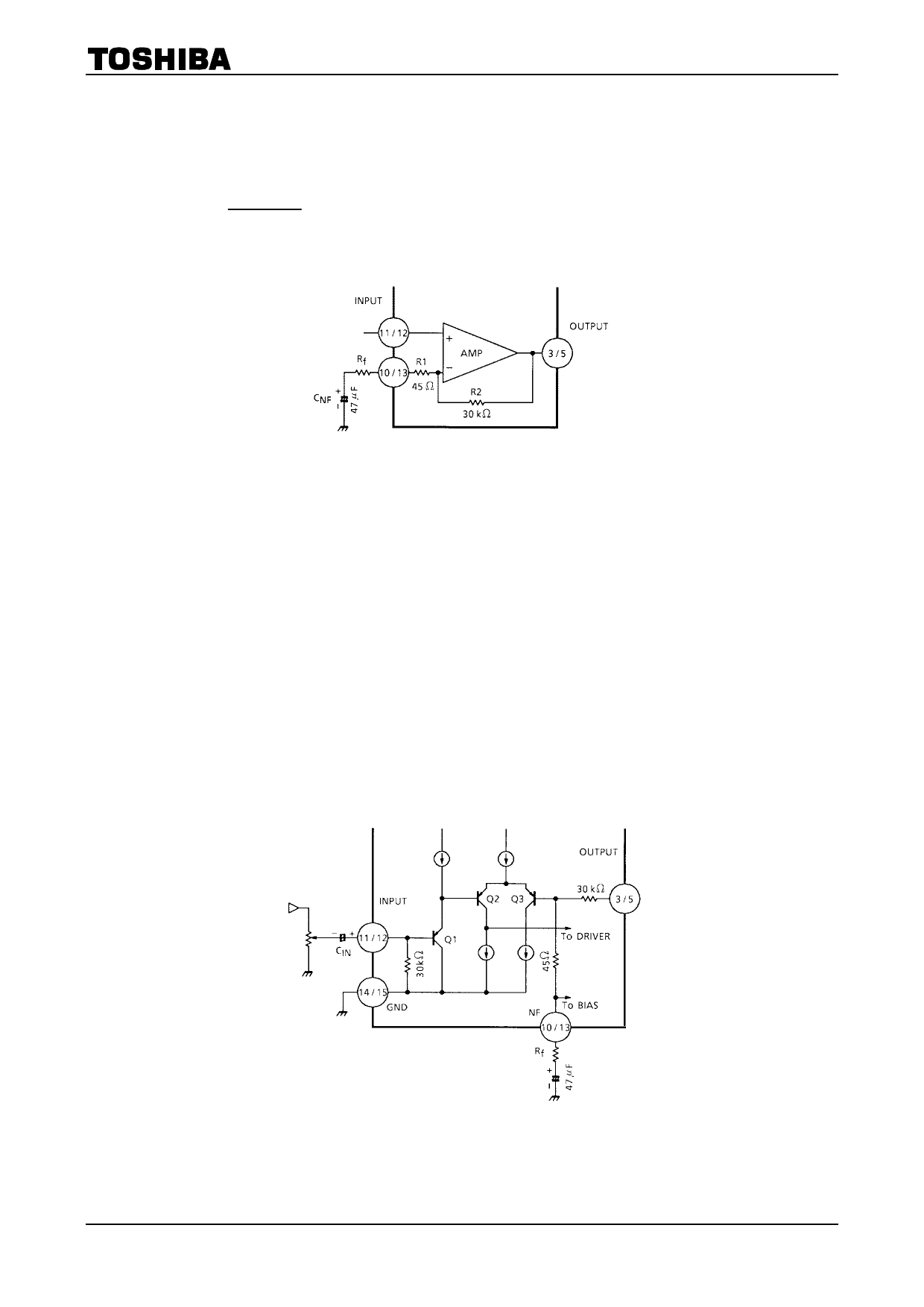
1. Adjustment of voltage gain
The voltage gain Gv is obtained as follows by R1, R2 and Rf in Fig.1.
Gv
=
20
log
Rf + R1 + R2
Rf + R1
When Rf = 0 Ω,
Gv = 56.5dB (typ.)
When Rf = 120 Ω, Gv = 45dB (typ.)
TA8248K
Figure 1
By increasing Rf, reduction of Gv is possible. However, since the feedback increase is liable to produce
oscillation, it is recommended to use this at 40dB or over.
2. Thermal shut-down circuit
The thermal shut-down circuit is built in for the purpose of preventing the destruction of IC due to the
abnormal temperature rise when the heat radiation is insufficient.
The operation temperature is set at radiation Fin temperature 175°C (typ.). At this temperature or over the
bias is interrupted to prevent the destruction of IC.
3. Input stage
The input circuit of this IC is as shown in Fig.2.
PNP Tr : Q1 is provided in the input circuit so as to make its usage possible without the input coupling
capacitor.
However, at pin11 and 12, max 60 mV offset voltage is produced.
Application after checking volume slide noise is recommended.
For cutting the volume slide noise, insert the input capacitor : CIN in series to interrupt the DC component.
Figure 2
3
2002-04-05
Share Link: 