TA8696F データシートの表示(PDF) - Toshiba
部品番号
コンポーネント説明
メーカー
TA8696F Datasheet PDF : 12 Pages
| |||
TA8696F
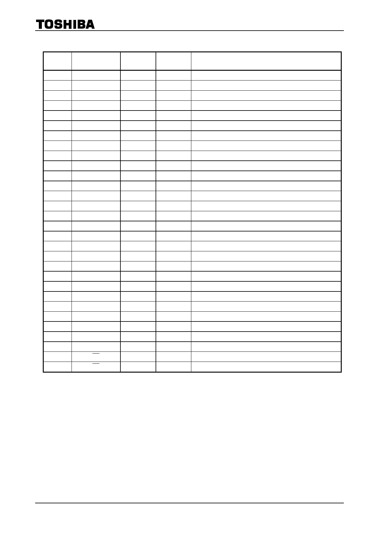
Pin Function
Pin No.
1
2
3
4
5
6
7
8
9
10
11
12
13
14
15
16
17
18
19
20
21
22
23
24
25
26
27
28
29
30
Pin Name
Mode Switch
CH B Input
CH G Input
CH R Input
BS/H
B Input
G Input
R Input
L.GND
RS/H
Vref
B Drive
R Drive
COM Drive
L.VCC
g Offset
COM Cut-off
R Cut-off
B Cut-off
H.GND
F.F. CONT.
R Output
G Output
B Output
VO Center
H.VCC
F.F. Output
CP
VD
HD
Reference
Voltage
(V)
0
0
0
0
1.6
1.6
1.6
1.6
0
1.6
1.6
2
2
2
4.0
2
2
2
2
0
1.4
6.5
6.5
6.5
6.5
13.0
0.2
0.9
1.4
0.9
Reference
Current
(mA)
0
0
0
0
0
0
0
0
-8.1
0
0
0
0
0
8.1
0
0
0
0
-4.6
¾
0
0
0
0
4.6
0
0
0
0
Function
CH display mode switching (latch mode/through mode)
CH display signal blue input
CH display signal green input
CH display signal red input
Blue input signal sample and hold capacitor
Blue primary color input
Green primary color input
Red primary color input
Low-voltage signal GND
Red input signal sample and hold capacitor
Internal reference voltage
B-axis drive control
R-axis drive control
Common drive control
Low-voltage signal VCC
g correction starting point control
Common cut-off control
R-axis cut-off control
B-axis cut-off control
High-voltage signal GND
¾
Red signal input
Green signal input
Blue signal input
Signal output center voltage control
High-voltage signal VCC
Flip-flop output
Clamp pulse input
Vertical drive pulse input
Horizontal drive pulse input
Note 1: Reference voltage and reference current are for DC bias with no signal.
The current which flows into the IC considered to be positive current.
2
2002-02-13
Share Link: 