TA8696F データシートの表示(PDF) - Toshiba
部品番号
コンポーネント説明
メーカー
TA8696F Datasheet PDF : 12 Pages
| |||
TA8696F
Pin No.
Pin Name and Function
Typical Signal Level
Internal bias
0V
Mode switch
Switches channel indication
mode
ViH = L.VCC
ViL = GND
1
High level: Character mode VTH = 1.9 V
Low level: Latch mode
ViH Max = L.VCC
(synchronized with HD)
ViL Min = GND
Clamped on L.VCC and GND
CH B input
Internal bias
0V
5V
2
CH G input
3
CH R input
0V
VTH = 1.7 V
4
Channel indication signal ViH Max = 5.5 V
Input pin
ViL Min = GND
Clamped on GND
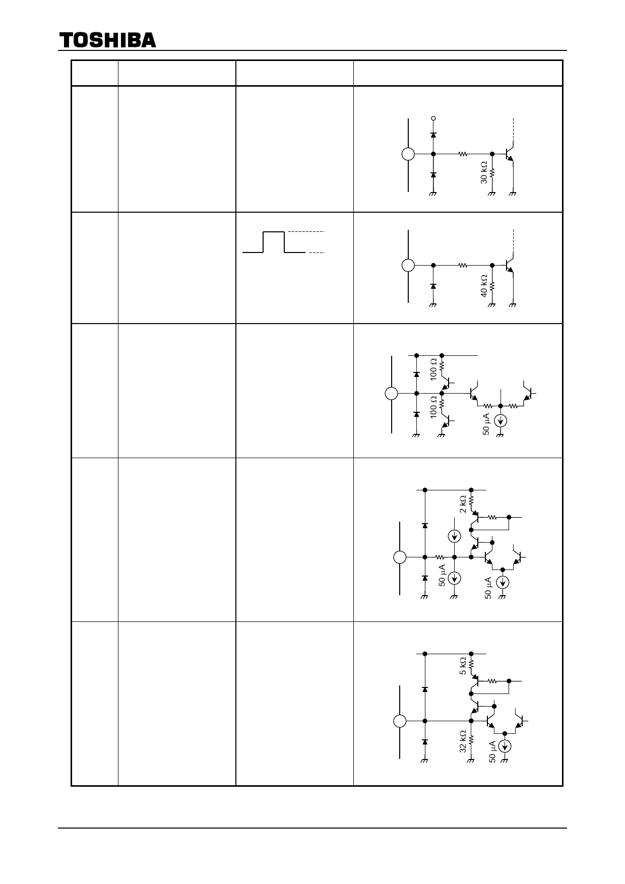
Interface Current
L.VCC
1
50 kW
2
3
60 kW
4
BS/H
Internal bias
1.6 V
5
RS/H
External capacitance 1 mF
10
Regenerate B/R-axis direct Permissible load current
current voltage
0
Capaciator pin
Clamped on L.VCC and GND
L.VCC
5
10
1 kW 1 kW
Internal bias
1.6 V
B input
6
White signal level 1.6 V
G input
7
Black signal level 0.9 V
R input
8
Primary color input pins
Maximum input level 1.4 Vp-p
Clamped on L.VCC and GND
L.VCC
6
14 kW
7
8
8 kW
Internal bias
1.6 V
11
Vref
Internal standard voltage
Permissible load current
0
reference pin
Clamped on L.VCC and GND
L.VCC
11
30 kW
3
2002-02-13
Share Link: 