RF2376 データシートの表示(PDF) - RF Micro Devices
部品番号
コンポーネント説明
メーカー
RF2376 Datasheet PDF : 10 Pages
| |||
RF2376
Preliminary
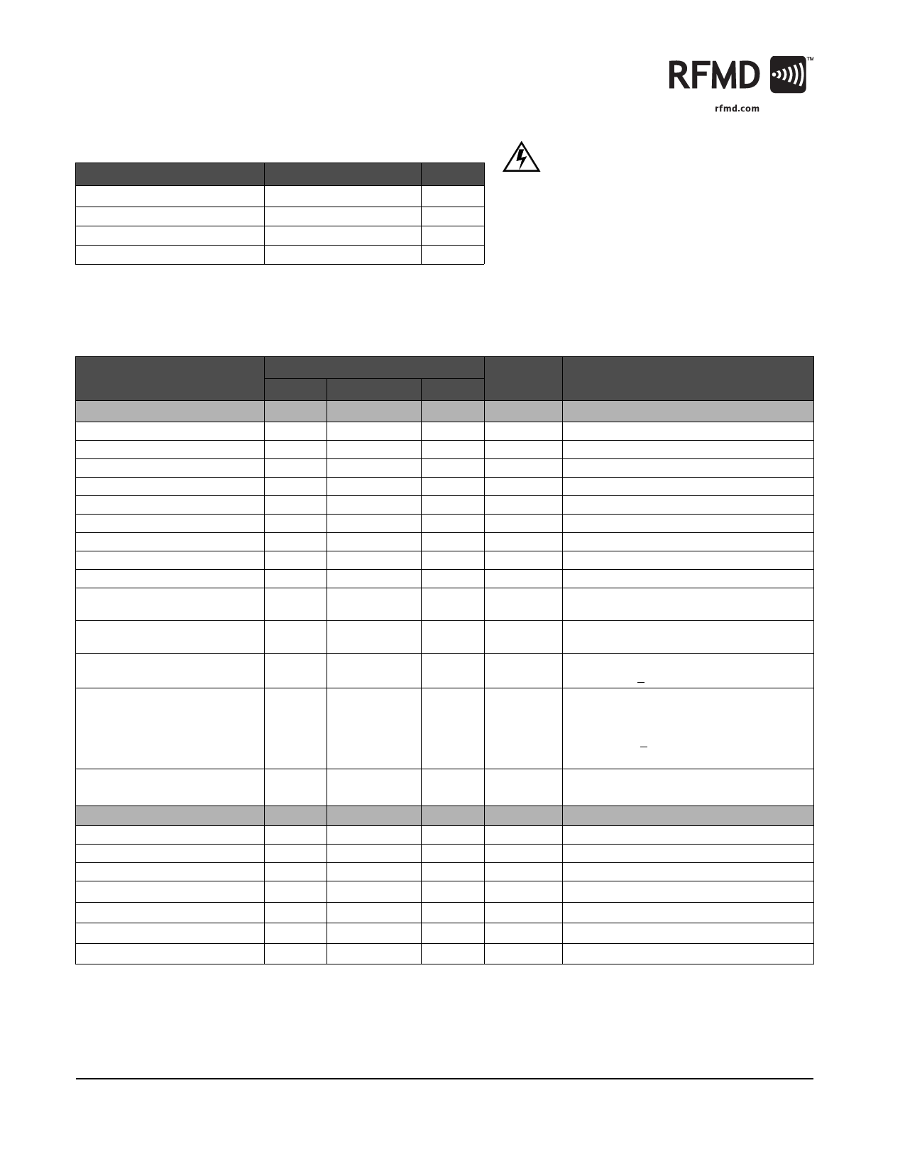
Absolute Maximum Ratings
Parameter
Supply Voltage
DC Current
Operating Ambient Temperature
Storage Temperature
Rating
0 to +5.0
100
-20 to +85
-40 to +150
Unit
VDC
mA
°C
°C
Caution! ESD sensitive device.
Exceeding any one or a combination of the Absolute Maximum Rating conditions may
cause permanent damage to the device. Extended application of Absolute Maximum
Rating conditions to the device may reduce device reliability. Specified typical perfor-
mance or functional operation of the device under Absolute Maximum Rating condi-
tions is not implied.
RoHS status based on EUDirective2002/95/EC (at time of this document revision).
The information in this publication is believed to be accurate and reliable. However, no
responsibility is assumed by RF Micro Devices, Inc. ("RFMD") for its use, nor for any
infringement of patents, or other rights of third parties, resulting from its use. No
license is granted by implication or otherwise under any patent or patent rights of
RFMD. RFMD reserves the right to change component circuitry, recommended appli-
cation circuitry and specifications at any time without prior notice.
Parameter
Overall
Operating Frequency
Usable Frequency Range
Maximum Small Signal Gain
Linear Gain Control Range
Gain Control Slope
Input VSWR
Output IP3
Noise Figure
Maximum Average Output Power
Adjacent Channel Power
Rejection
Alternate Channel Power
Rejection
Maximum Average Output Power
Adjacent Channel Power
Rejection
Specification
Min.
Typ.
Max.
836
800 to >1000
24
27
30
50
70
1.5:1
2.5:1
+22
+25
7
+8
-33
-32
-61
-57
+10
-53
Alternate Channel Power
Rejection
Power Supply
Supply Voltage
Gain Control Voltage
Supply Current
VGC Current
-67
2.8
2.7 to 3.3
0 to 2.0
25
30
40
34
18
1.5
Unit
MHz
MHz
dB
dB
dB/V
dBm
dB
dBm
dBc
dBc
dBm
dBc
dBc
V
V
V
mA
mA
mA
mA
Condition
VCC=2.8V, VGC=2.0V, T=25°C
Maximum gain.
Over entire gain control range
Maximum gain
TDMA modulation
TDMA modulation; POUT=+8dBm
TDMA modulation; POUT=+8dBm
CDMA modulation; VCC=3.0V, maximum gain
setting, ACPR<-52dBc.
CDMA modulation; VCC=3.0V. For
PIN>-23dBm, adjustment of PIN is required to
maintain ACPR performance over gain control
range. For PIN< -23dBm, ACPR performance is
maintained over entire gain control range.
CDMA modulation; POUT=+10dBm,
VCC = 3.0 V.
T = 25°C
Specifications
Operating range
VCC=2.8V, VGC=2.0V
VCC=3.0V, VGC=2.0V
VCC=2.8V, VGC=0.4V
2 of 10
7628 Thorndike Road, Greensboro, NC 27409-9421 · For sales or technical
support, contact RFMD at (+1) 336-678-5570 or sales-support@rfmd.com.
Rev A2 DS010829
Share Link: 