TC110 データシートの表示(PDF) - Microchip Technology
部品番号
コンポーネント説明
メーカー
TC110 Datasheet PDF : 16 Pages
| |||
TC110
1.0 ELECTRICAL
CHARACTERISTICS
Absolute Maximum Ratings*
Voltage on VDD, VOUT, SHDN Pins ........ -0.3V to +12V
EXT Output Current ................................... ±100mA pk
Voltage on EXT Pin ........................-0.3V to VDD +0.3V
Power Dissipation.............................................150mW
Operating Temperature Range............. -40°C to +85°C
Storage Temperature Range .............. -40°C to +125°C
*Stresses above those listed under "Absolute Maximum
Ratings" may cause permanent damage to the device. These
are stress ratings only and functional operation of the device
at these or any other conditions above those indicated in the
operation sections of the specifications is not implied.
Exposure to Absolute Maximum Rating conditions for
extended periods may affect device reliability.
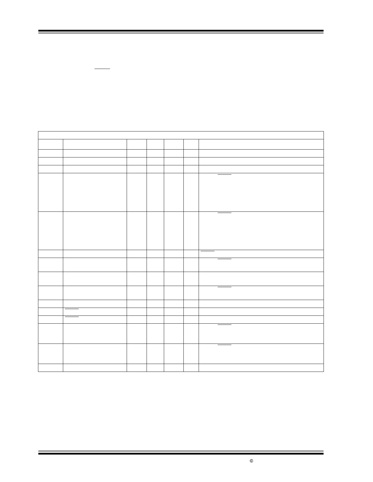
TC110 ELECTRICAL SPECIFICATIONS
Electrical Characteristics: Note 1, VIN = 0.6 x VR, VDD = VOUT, TA = 25°C, unless otherwise noted.
Symbol
Parameter
Min Typ Max Units
Test Conditions
VDD
Operating Supply Voltage
2.0
VSTART Start-Up Supply Voltage
—
VHOLD-UP Oscillator Hold-Up Voltage
—
IDD
Boost Mode Supply Current —
—
—
—
—
—
ISTBY
Standby Supply Current
—
—
—
—
—
—
ISHDN
Shutdown Supply Current
—
fOSC
Oscillator Frequency
255
85
VOUT
Output Voltage
VR
x 0.975
—
—
—
120
130
180
50
50
70
20
20
22
11
11
11
0.05
300
100
VR
10.0
0.9
0.7
190
200
280
90
100
120
34
35
38
20
20
22
0.5
345
115
VR
x 1.025
V Note 2
V IOUT = 1mA
V IOUT = 1mA
µA VOUT = SHDN = (0.95 x VR); fOSC = 300kHz; VR = 3.0V
VR = 3.3V
VR = 5.0V
fOSC = 100kHz; VR = 3.0V
VR = 3.3V
VR = 5.0V
µA VOUT = SHDN = (VR + 0.5V); fOSC = 300kHz; VR = 3.0V
VR = 3.3V
VR = 5.0V
fOSC = 100kHz; VR = 3.0V
VR = 3.3V
VR = 5.0V
µA SHDN = GND, VO = (VR x 0.95)
kHz VOUT = SHDN = (0.95 x VR); fOSC = 300kHz
fOSC = 100kHz
V Note 3
DTYMAX Maximum Duty Cycle
(PWM Mode)
—
—
92
% VOUT = SHDN = 0.95 x VR
DTYPFM Duty Cycle (PFM Mode)
15
25
35
% IOUT = 0mA
VIH
SHDN Input Logic High
0.65 —
—
V VOUT = (VR x 0.95)
VIL
SHDN Input Logic Low
—
— 0.20 V VOUT = (VR x 0.95)
REXTH EXT ON Resistance to VDD —
32
47
Ω VOUT = SHDN = (VR x 0.95); VR = 3.0V
—
29
43
VR = 3.3V
—
20
29
VEXT = (VOUT – 0.4V)
VR = 5.0V
REXTL EXT ON Resistance to GND —
20
30
Ω VOUT = SHDN = (VR x 0.95); VR = 3.0V
—
19
27
VR = 3.3V
—
13
19
VEXT = 0.4V
VR = 5.0V
η
Efficiency
—
84
—
%
Note
1: VR = 3.0V, IOUT = 120mA
VR = 3.3V, IOUT = 130mA
VR = 5.0V, IOUT = 200mA
2: See Application Notes “Operating Mode” description for clarification.
3: VR is the factory output voltage setting.
DS21355B-page 2
© 2002 Microchip Technology Inc.
Share Link: 