TC115 データシートの表示(PDF) - Microchip Technology
部品番号
コンポーネント説明
メーカー
TC115 Datasheet PDF : 14 Pages
| |||
TC115
1.0 ELECTRICAL
CHARACTERISTICS
Absolute Maximum Ratings*
Power Supply Voltage (PS) .................................... 12V
Power Dissipation.............................................500mW
LX Sink Current ............................................ 400mA pk
SHDN Input Voltage ............................................... 12V
Operating Temperature Range............. -40°C to +85°C
Storage Temperature Range .............. -40°C to +125°C
*Stresses above those listed under "Absolute Maximum
Ratings" may cause permanent damage to the device. These
are stress ratings only and functional operation of the device
at these or any other conditions above those indicated in the
operation sections of the specifications is not implied.
Exposure to Absolute Maximum Rating conditions for
extended periods may affect device reliability.
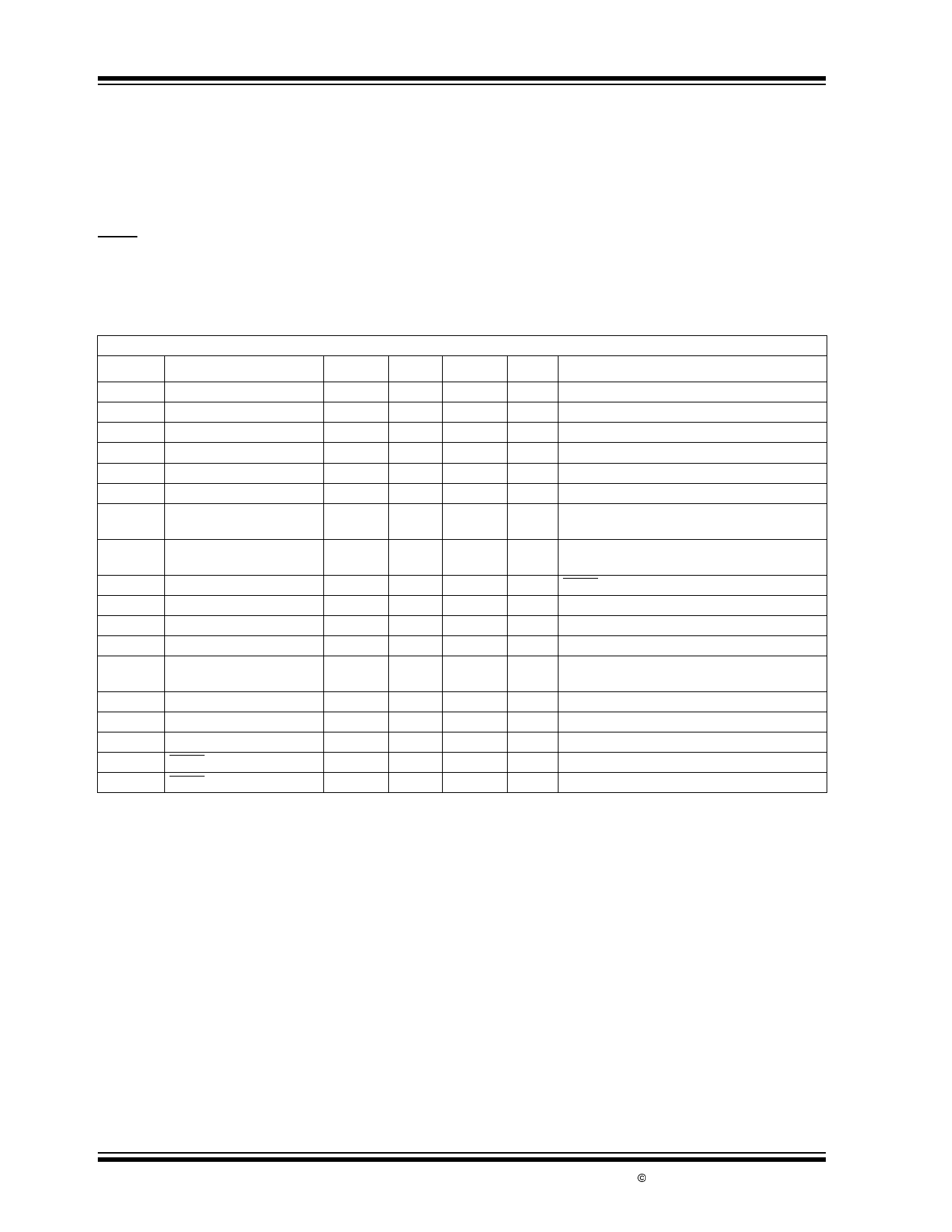
TC115 ELECTRICAL SPECIFICATIONS
Electrical Characteristics: VOUT = 5V, TA = 25°C, unless otherwise noted. Circuit configuration per Figure 4-1.
Symbol
Parameter
Min
Typ
Max Units
Test Conditions
VIN
Operating Supply Voltage
0.9
—
10.0
V Note 5
VSTART Start-Up Supply Voltage
—
—
0.9
V IOUT = 1mA
ILXMAX
LX Maximum Sink Current
—
—
350
mA
fLIM
LX Limit Frequency
—
200
—
kHz VLX = VLXLIM
VLXLIM LX Limit Voltage
0.7
—
1.3
V Note 2
IDD
No Load Supply Current
—
13
26
µA IOUT = 0, VIN = VOUT x 0.8 (Note3)
ICC
Boost Mode Supply Current —
80
135
µA No external components,
VIN = (0.95 x VOUT) applied to PS (or VDD) input
ISTBY
Standby Supply Current
—
9
17
µA No external components,
VIN = (1.1 x VOUT) applied to PS (or VDD) input
ISD
Shutdown Supply Current
—
—
0.5
µA SHDN = 0V
fOSC
Oscillator Frequency
85
100
115
kHz Note 2, Note 4
VOUT
Output Voltage
VR x 0.975 VR VR x 1.025 V VIN = 2.2V minimum (Note 1)
RSWON LX Output ON Resistance
—
1.4
2.4
Ω VLX = 0.4V
PFMDUTY Duty Cycle
10
17
25
% No external components.
(PFM Operating Mode)
MAXDUTY Maximum Duty Cycle
80
87
92
% Note 4
tSS
Soft Start Time
η
Efficiency
4
10
20
msec
—
85
—
%
VIH
VIL
Note
SHDN Input Logic High
0.75
—
—
V
SHDN Input Logic Low
—
—
0.20
V
1: VR is the nominal factory-programmed output voltage setting.
2: VLXLIM is the voltage on the LX pin (with internal switch ON) that will cause the oscillator to run at twice nominal frequency in to limit the
switch current through the internal N-channel switching transistor.
3: Measured with D1 = MA735 (reverse current < 1µA at a reverse voltage of 10V).
4: With TC115 operating in PWM mode.
5: See Section 3.4 “Behavior When VIN is Greater Than the Factory-Programmed VOUT Setting”.
DS21361B-page 2
© 2002 Microchip Technology Inc.
Share Link: 