TC115 データシートの表示(PDF) - Microchip Technology
部品番号
コンポーネント説明
メーカー
TC115 Datasheet PDF : 14 Pages
| |||
TC115
Re-writing in terms of input and output currents and
voltages:
EQUATION 4-5:
(VINMIN) (IINMAX) =
(VOUTMAX) (IOUTMAX)
Efficiency
Solving for input curent:
EQUATION 4-6:
IINMAX =
(VOUTMAX) (IOUTMAX)
(Efficiency) (VINMAX)
The sawtooth current is centered on the DC current
level; swinging equally above and below the DC current
calculated in Equation 4-6. The peak inductor current is
the sum of the DC current plus half the AC current.
Note that minimum input voltage should be used when
calculating the AC inductor current (Equation 4-9).
EQUATION 4-7:
V
=
L(di)
dt
EQUATION 4-8:
di
=
V(dt)
dt
EQUATION 4-9:
di = [(VINMIN – VSW)tON]
L
where: VSW = The voltage drop across the internal
N-channel MOSFET.
Combining the DC current calculated in Equation 4-6,
with half the peak AC current calculated in Equation 4-
9, the peak inductor current is given by:
EQUATION 4-10:
IPK = IINMAX + 0.5(di)
4.3 Internal Transistor Switch
The LX pin has a typical ON resistance of 1.4Ω,
therefore peak switch current is given by (VIN/1.4). The
internal transistor switch has a maximum design rating
of 350mA. An oscillator frequency doubling circuit is an
included guard against high switching currents. Should
the voltage on the LX pin rise above 1.3V, max, while
the internal N-channel switch is ON, the oscillator
frequency automatically doubles to minimize ON time.
Although reduced, switch current still flows because
the PWM remains in operation. Therefore, the LX input
is not internally current limited and care must be taken
never to exceed the 350mA maximum limit. Failure to
observe this will result in damage to the regulator.
4.4 Output Capacitor
The effective series resistance of the output capacitor
directly affects the amplitude of the output voltage
ripple. (The product of the peak inductor current and
the ESR determines output ripple amplitude.) There-
fore, a capacitor with the lowest possible ESR should
be selected. Smaller capacitors are acceptable for light
loads or in applications where ripple is not a concern.
The Sprague 595D series of tantalum capacitors are
among the smallest of all low ESR surface mount
capacitors available. Table 4-1 lists suggested
components and suppliers.
4.5 Board Layout Guidelines
As with all inductive switching regulators, the TC115
generates fast switching waveforms which radiate
noise. Interconnecting lead lengths should be
minimized to keep stray capacitance, trace resistance
and radiated noise as low as possible. In addition, the
GND pin, input bypass capacitor and output filter
capacitor ground leads should be connected to a single
point. The input capacitor should be placed as close to
power and ground pins of the TC115 as possible.
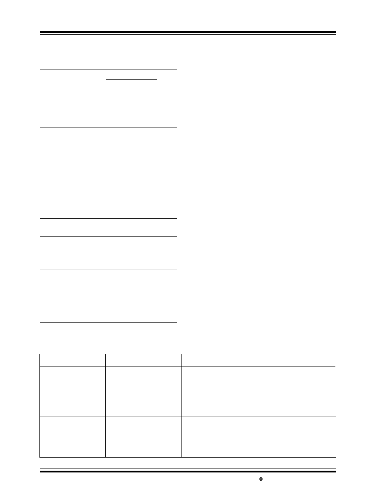
TABLE 4-1: SUGGESTED COMPONENTS AND SUPPLIERS
Type
Surface Mount
Through-Hole
Inductors
Sumida
CD54 Series
CDR125 Series
Coiltronics
CTX Series
Sumida
RCH855 Series
RCH110 Series
Renco
RL1284-12
Capacitors
Matsuo
267 Series
Sprague
595D Series
Nichicon
F93 Series
Sanyo
OS-CON Series
Nichicon
PL Series
Diodes
Nihon
EC10 Series
Matsushita
MA735 Series
ON Semiconductor
1N5817 - 1N5822
DS21361B-page 6
© 2002 Microchip Technology Inc.
Share Link: 