TC1073-28VCH データシートの表示(PDF) - Microchip Technology
部品番号
コンポーネント説明
メーカー
TC1073-28VCH
Microchip Technology

TC1073-28VCH Datasheet PDF : 20 Pages
| |||
TC1072/TC1073
1.0 ELECTRICAL
CHARACTERISTICS
Absolute Maximum Ratings*
Input Voltage......................................................... 6.5V
Output Voltage ...........................(-0.3V) to (VIN + 0.3V)
Power Dissipation ............... Internally Limited (Note 6)
Maximum Voltage on Any Pin ........ VIN +0.3V to -0.3V
Operating Temperature Range ......-40°C < TJ < 125°C
Storage Temperature ......................... -65°C to +150°C
*Stresses above those listed under "Absolute Maximum
Ratings" may cause permanent damage to the device. These
are stress ratings only and functional operation of the device
at these or any other conditions above those indicated in the
operation sections of the specifications is not implied.
Exposure to Absolute Maximum Rating conditions for
extended periods may affect device reliability.
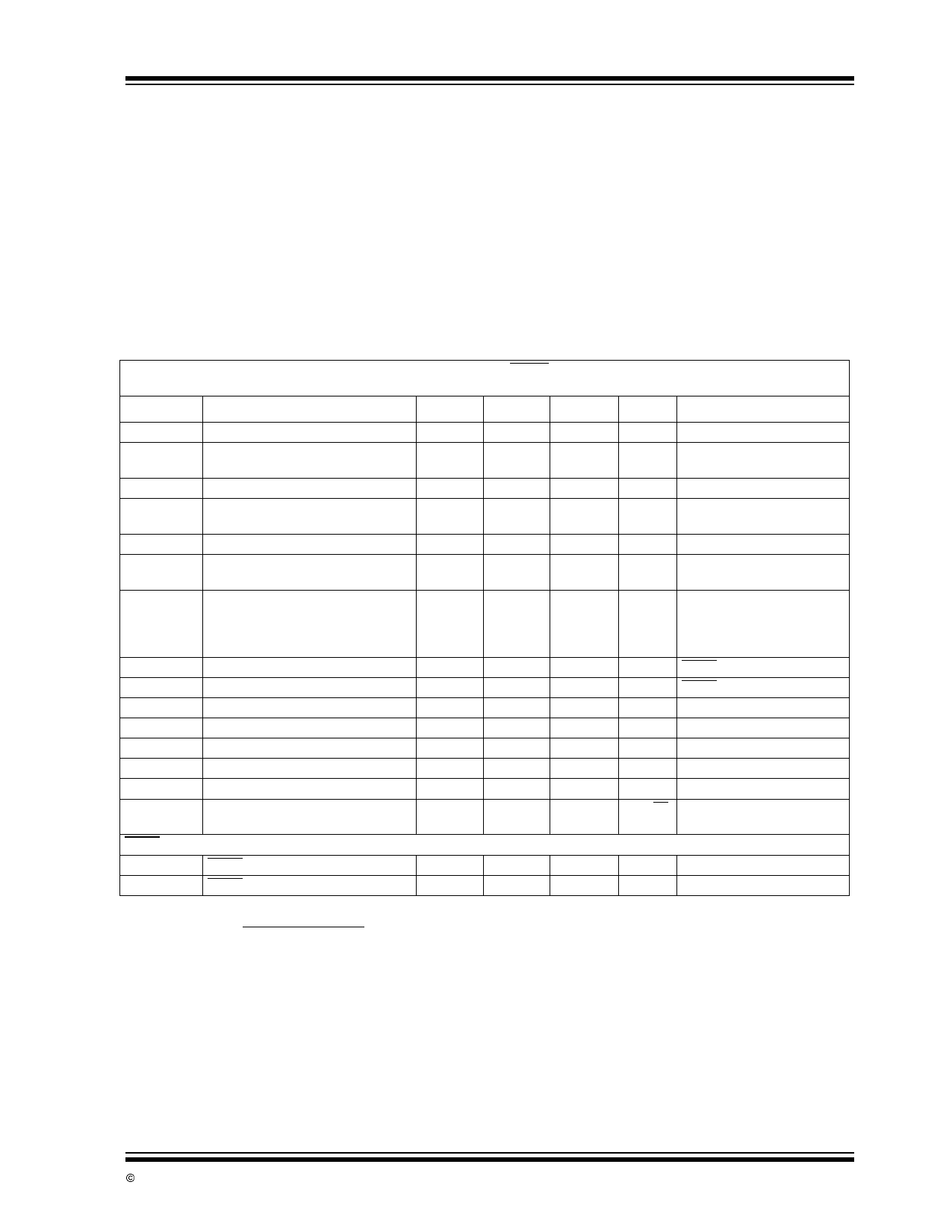
TC1072/TC1073 ELECTRICAL SPECIFICATIONS
Electrical Characteristics: VIN = VOUT + 1V, IL = 0.1mA, CL = 3.3µF, SHDN > VIH, TA = 25°C, unless otherwise noted. Boldface
type specifications apply for junction temperatures of -40°C to +125°C.
Symbol
Parameter
Min
Typ
Max
Units
Test Conditions
VIN
IOUTMAX
Input Operating Voltage
Maximum Output Current
2.7
—
50
—
100
—
6.0
V Note 9
—
mA TC1072
—
mA TC1073
VOUT
TCVOUT
Output Voltage
VOUT Temperature Coefficient
VR – 2.5%
—
—
VR ±0.5%
20
40
VR + 2.5%
—
—
V
ppm/°C
Note 1
Note 2
∆VOUT/∆VIN Line Regulation
∆VOUT/VOUT Load Regulation
—
0.05
0.35
% (VR + 1V) ≤ VIN ≤ 6V
—
0.5
2.0
%
IL = 0.1mA to IOUTMAX
(Note 3)
VIN-VOUT
Dropout Voltage
—
—
—
—
IIN
Supply Current
—
IINSD
Shutdown Supply Current
—
PSRR
Power Supply Rejection Ratio
—
IOUTSC
Output Short Circuit Current
—
∆VOUT/∆PD Thermal Regulation
—
TSD
Thermal Shutdown Die Temperature
—
∆TSD
Thermal Shutdown Hysteresis
—
eN
Output Noise
—
2
65
85
180
50
0.05
64
300
0.04
160
10
260
—
mV IL = 0.1mA
—
IL = 20mA
120
IL = 50mA
250
IL = 100mA (Note 4), TC1073
80
µA SHDN = VIH, IL = 0 (Note 8)
0.5
µA SHDN = 0V
—
dB FRE ≤ 1kHz
450
mA VOUT = 0V
—
V/W Notes 5, 6
—
°C
—
°C
—
nV/√Hz IL = IOUTMAX
470pF from Bypass to GND
SHDN Input
VIH
SHDN Input High Threshold
45
—
—
%VIN VIN = 2.5V to 6.5V
VIL
SHDN Input Low Threshold
—
—
15
%VIN VIN = 2.5V to 6.5V
Note 1: VR is the regulator output voltage setting. For example: VR = 2.5V, 2.7V, 2.85V, 3.0V, 3.3V, 3.6V, 4.0V, 5.0V.
2: TC VOUT = (VOUTMAX – VOUTMIN) x 106
VOUT x ∆T
3: Regulation is measured at a constant junction temperature using low duty cycle pulse testing. Load regulation is tested over a load range
from 0.1mA to the maximum specified output current. Changes in output voltage due to heating effects are covered by the thermal
regulation specification.
4: Dropout voltage is defined as the input to output differential at which the output voltage drops 2% below its nominal value.
5: Thermal Regulation is defined as the change in output voltage at a time T after a change in power dissipation is applied, excluding load or
line regulation effects. Specifications are for a current pulse equal to ILMAX at VIN = 6V for T = 10 msec.
6: The maximum allowable power dissipation is a function of ambient temperature, the maximum allowable junction temperature and the
thermal resistance from junction-to-air (i.e., TA, TJ, θJA). Exceeding the maximum allowable power dissipation causes the device to initiate
thermal shutdown. Please see Section 4.0 Thermal Considerations for more details.
7: Hysteresis voltage is referenced by VR.
8: Apply for Junction Temperatures of -40°C to +85°C.
9: The minimum VIN has to justify the conditions = VIN ≥ VR + VDROPOUT and VIN ≥ 2.7V for IL = 0.1mA to IOUTMAX.
© 2002 Microchip Technology Inc.
DS21354B-page 3
Share Link: