LC7470 データシートの表示(PDF) - SANYO -> Panasonic
部品番号
コンポーネント説明
メーカー
LC7470 Datasheet PDF : 13 Pages
| |||
LC7470
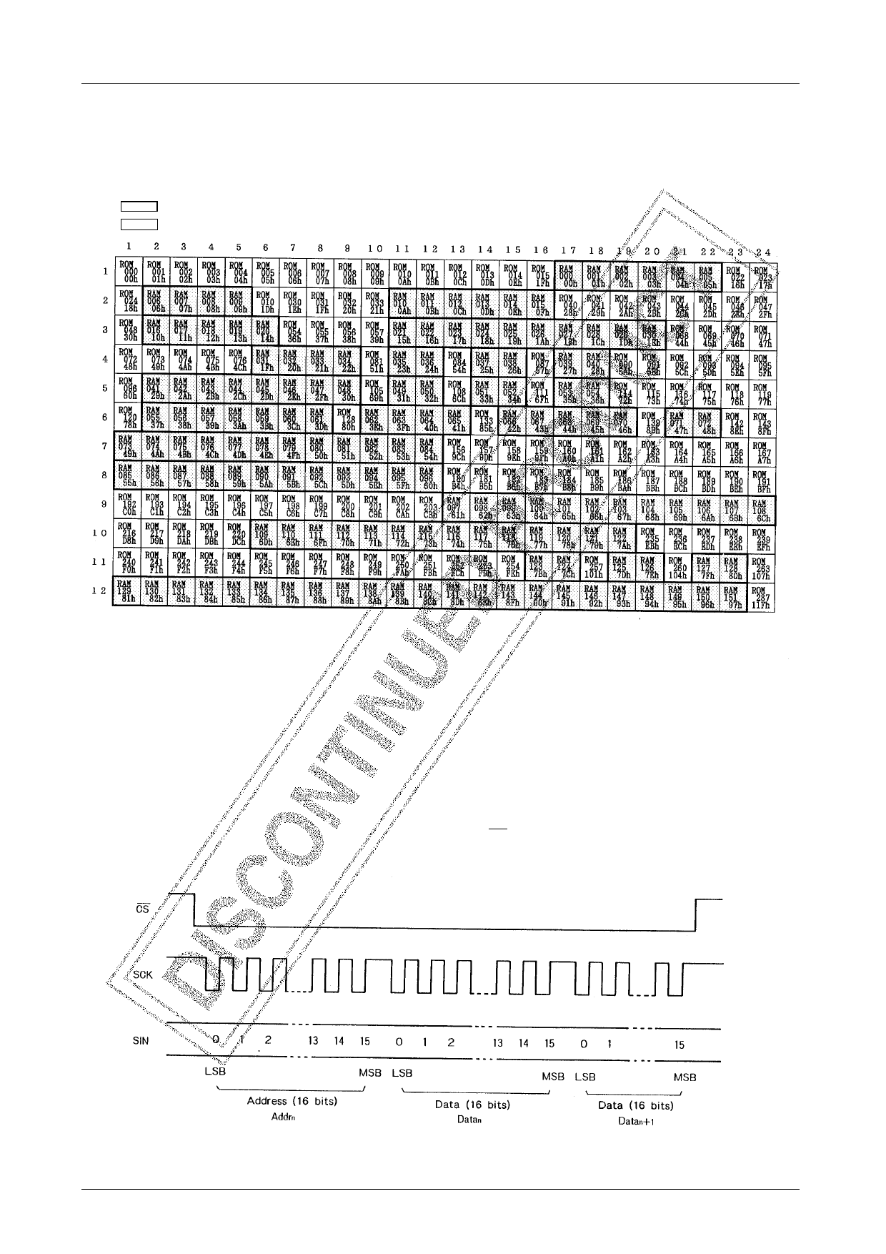
Sample Display Screen
Twelve display lines of the display 64-line ROM are specified. Variable characters are prepared in the display control
RAM. The display RAM address area is automatically allocated to addresses from 0D (000H) to 175D (AFH) in the
display order.
The display characters indicated by bold lines are specified through the display RAM access.
The display characters indicated by slender lines are specified directly through the display ROM access.
Input Timings of External Control Data
Address and data information is input serially to this chip from an external device.
(1) Address data consist of 16 bits.
The 8 low-order bits have significance. Always set 8 high-order bits to ‘0’.
(2) Data consists of 16 bits.
• Only 8 low-order bits of input data to addresses from 000H to 0AFH have significance. Always set 8 high-order bits
to ‘0’.
• Only 11 low-order bits of input data to addresses from 0B0H to 0BBH have significance. Always set 5 high-order
bits to ‘0’.
• Only 12 low-order bits of input data to addresses from 0BCH to 0BFH have significance. Always set 4 high-order
bits to ‘0’.
(3) The data input format is shown below. The first 16 bits after the CS pin (active low) becomes active are processes as
an address data. The subsequent groups of 16 bits are handled as the data.
No.3725–11/13
Share Link: 