TC72(2011) データシートの表示(PDF) - Microchip Technology
部品番号
コンポーネント説明
メーカー
TC72 Datasheet PDF : 28 Pages
| |||
TC72
1.0 ELECTRICAL
CHARACTERISTICS
1.1 Maximum Ratings†
VDD........................................................................ 6.0V
All inputs and outputs w.r.t. GND ...-0.3V to VDD +0.3V
Storage temperature .......................... -65°C to +150°C
Ambient temp. with power applied ..... -55°C to +125°C
Junction Temperature ........................................ 150°C
ESD protection on all pins:
Human Body Model (HBM)............................. > 4 kV
Man Machine Model (MM)............................. > 400V
Latch-Up Current at each pin ........................ ±200 mA
Maximum Power Dissipation........................... 250 mW
† Notice: Stresses above those listed under "Maximum
Ratings" may cause permanent damage to the device. This is
a stress rating only and functional operation of the device at
those or any other conditions above those indicated in the
operation listings of this specification is not implied. Exposure
to maximum rating conditions for extended periods may affect
device reliability.
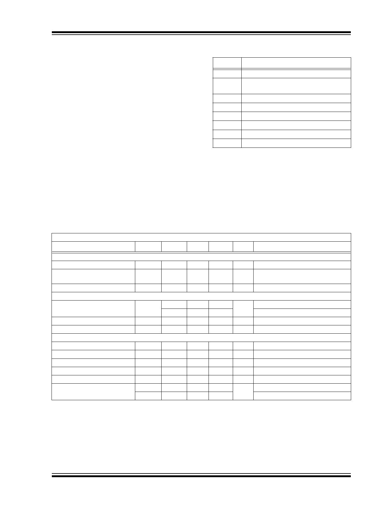
DC CHARACTERISTICS
Electrical Specifications: Unless otherwise noted, all parameters apply at VDD = 2.65V to 5.5V,
TA = -55°C to +125°C.
Parameters
Sym Min Typ Max Units
Conditions
Power Supply
Operating Voltage Range
VDD
2.65 —
5.5
Operating Current:
IDD-CON
—
Normal Mode, ADC Active
250 400
V Note 1
µA Continuous Temperature Conversion
mode (Shutdown Bit = ‘0’)
Shut-Down Supply Current
ISHD
—
0.1 1.0
Temperature Sensor and Analog-to-Digital Converter
µA Shutdown mode (Shutdown Bit = ‘1’)
Temperature Accuracy
(Note 1)
Resolution
TACY
-2.0
— +2.0
°C -40°C < TA < +85°C
-3.0 — +3.0
-55°C < TA < +125°C
—
10
—
Bits Note 4
ADC Conversion Time
Digital Input / Output
tCONV
— 150 200 ms
High Level Input Voltage
VIH 0.7 VDD —
—
V
Low Level Input Voltage
VIL
—
— 0.2 VDD V
High Level Output Voltage
VOH 0.7 VDD —
—
V IOH = 1 mA
Low Level Output Voltage
VOL
—
— 0.2 VDD V IOL = 4 mA
Input Resistance
RIN
1.0
—
—
MΩ
Pin Capacitance
CIN
—
15
—
pF
COUT
—
50
—
Note 1: The TC72-2.8MXX, TC72-3.3MXX and TC72-5.0MXX will operate from a supply voltage of 2.65V to 5.5V.
However, the TC72-2.8MXX, TC72-3.3MXX and TC72-5.0MXX are tested and specified at the nominal
operating voltages of 2.8V, 3.3V and 5.0V respectively. As VDD varies from the nominal operating value,
the accuracy may be degraded. Refer to Figure 2-5 and Figure 2-6.
2: Measured with a load of CL = 50 pF on the SDO output pin of the TC72.
3: All time measurements are measured with respect to the 50% point of the signal, except for the SCK rise
and fall times. The rise and fall times are defined as the 10% to 90% transition time.
4: Resolution = Temperature Range/No. of Bits = (+127°C – -128°C) / (210) = 256/1024 = 0.25°C/Bit
© 2011 Microchip Technology Inc.
DS21743B-page 3
Share Link: 