M80C186 データシートの表示(PDF) - Intel
部品番号
コンポーネント説明
メーカー
M80C186 Datasheet PDF : 59 Pages
| |||
M80C186
Symbol
TMR IN 0
TMR IN 1
TMR OUT 0
TMR OUT 1
DRQ0
DRQ1
NMI
INT0 INT1
INT2 INTA0
INT3 INTA1
A19 S6
A18 S5
A17 S4
A16 S3
AD15
AD14
AD13
AD12
AD11
AD10
AD9
AD8
AD7
AD6
AD5
AD4
AD3
AD2
AD1
AD0
PGA
20
21
22
23
18
19
46
45 44
42
41
65
66
67
68
1
3
5
7
10
12
14
16
2
4
6
8
11
13
15
17
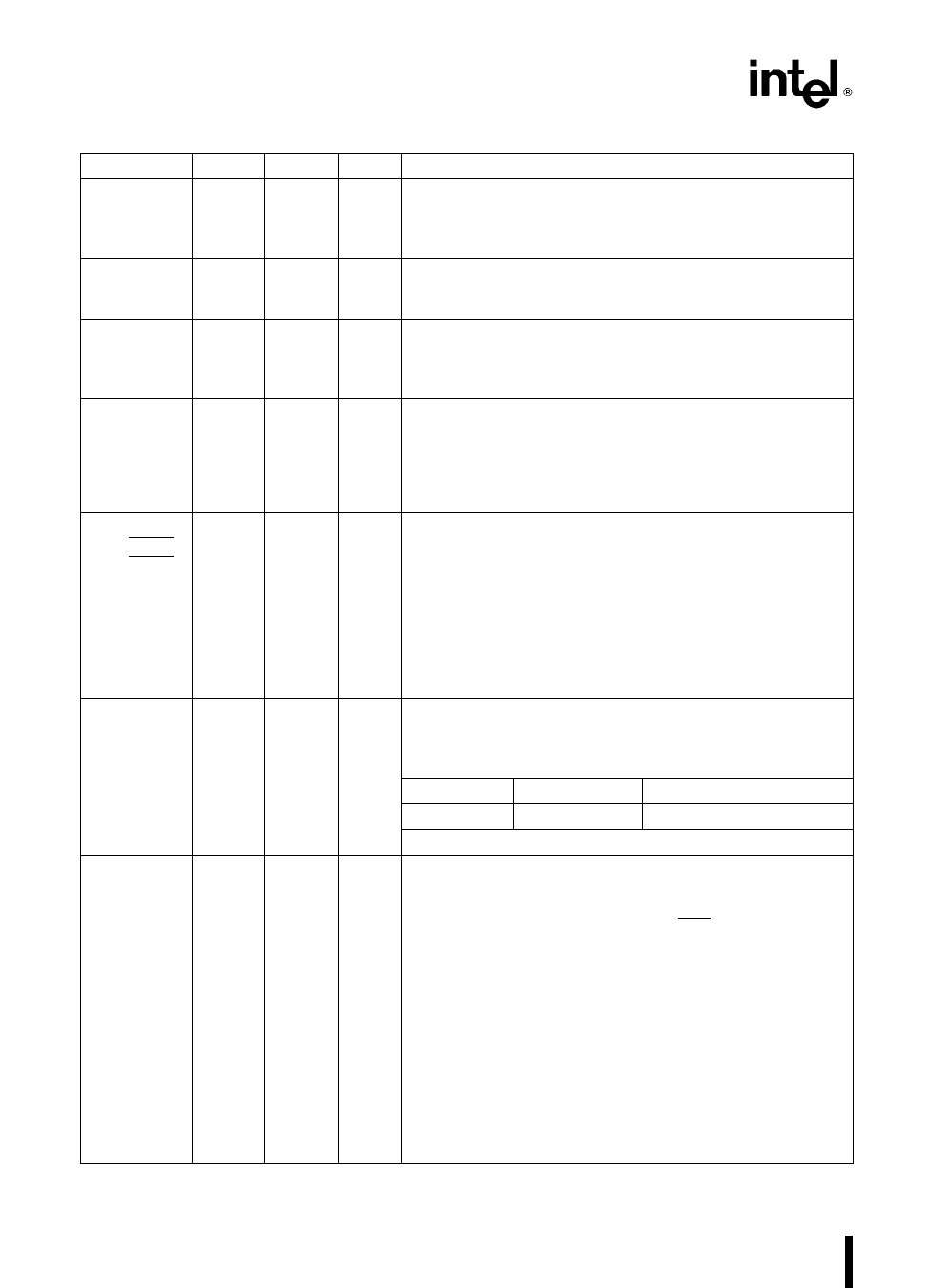
Table 1 M80C186 Pin Description (Continued)
QFP Type
Name and Function
58
I Timer Inputs are used either as clock or control signals
57
I depending upon the programmed timer mode These inputs
are active HIGH (or LOW-to-HIGH transitions are counted) and
internally synchronized
56
O Timer outputs are used to provide single pulse or continous
55
O waveform generation depending upon the timer mode
selected
60
I DMA Request is driven HIGH by an external device when it
59
I desires that a DMA channel (Channel 0 or 1) perform a
transfer These signals are active HIGH level-triggered and
internally synchronized
32
I Non-Maskable Interrupt is an edge-triggered input which
causes a type 2 interrupt NMI is not maskable internally A
transition from a LOW to HIGH initiates the interrupt at the
next instruction boundary NMI is latched internally An NMI
duration of one clock or more will guarantee service This input
is internally synchronized
33 34
36
37
I Maskable Interrupt Requests can be requested by activating
I O one of these pins When configured as inputs these pins are
I O active HIGH Interrupt Requests are synchronized internally
INT2 and INT3 may be configured via software to provide
active-LOW interrupt-acknowledge output signals All interrupt
inputs may be configured via software to be either edge- or
level-triggered To ensure recognition all interrupt requests
must remain active until the interrupt is acknowledged When
slave mode is selected the function of these pins changes
(see Interrupt Controller section of this data sheet)
13
O Address Bus Outputs (16 – 19) and Bus Cycle Status (3 – 6)
12
O reflect the four most significant address bits during T1 These
11
O signals are active HIGH During T2 T3 TW and T4 status
10
O information is available on these lines as encoded below
Low
High
S6
Processor Cycle
DMA Cycle
S3 S4 and S5 are defined as LOW during T2 – T4
9
I O Address Data Bus (0 – 15) signals constitute the time
7
multiplexed memory or I O address (T1) and data (T2 T3 TW
5
and T4) bus The
3
bus is active HIGH A0 is analogous to BHE for the lower byte
68
of the data bus pins D7 through D0 It is LOW during T1 when
66
a byte is to be transferred onto the lower portion of the bus in
64
memory or I O operations
62
8
6
4
2
67
65
63
61
4
Share Link: 