M80C186 データシートの表示(PDF) - Intel
部品番号
コンポーネント説明
メーカー
M80C186 Datasheet PDF : 59 Pages
| |||
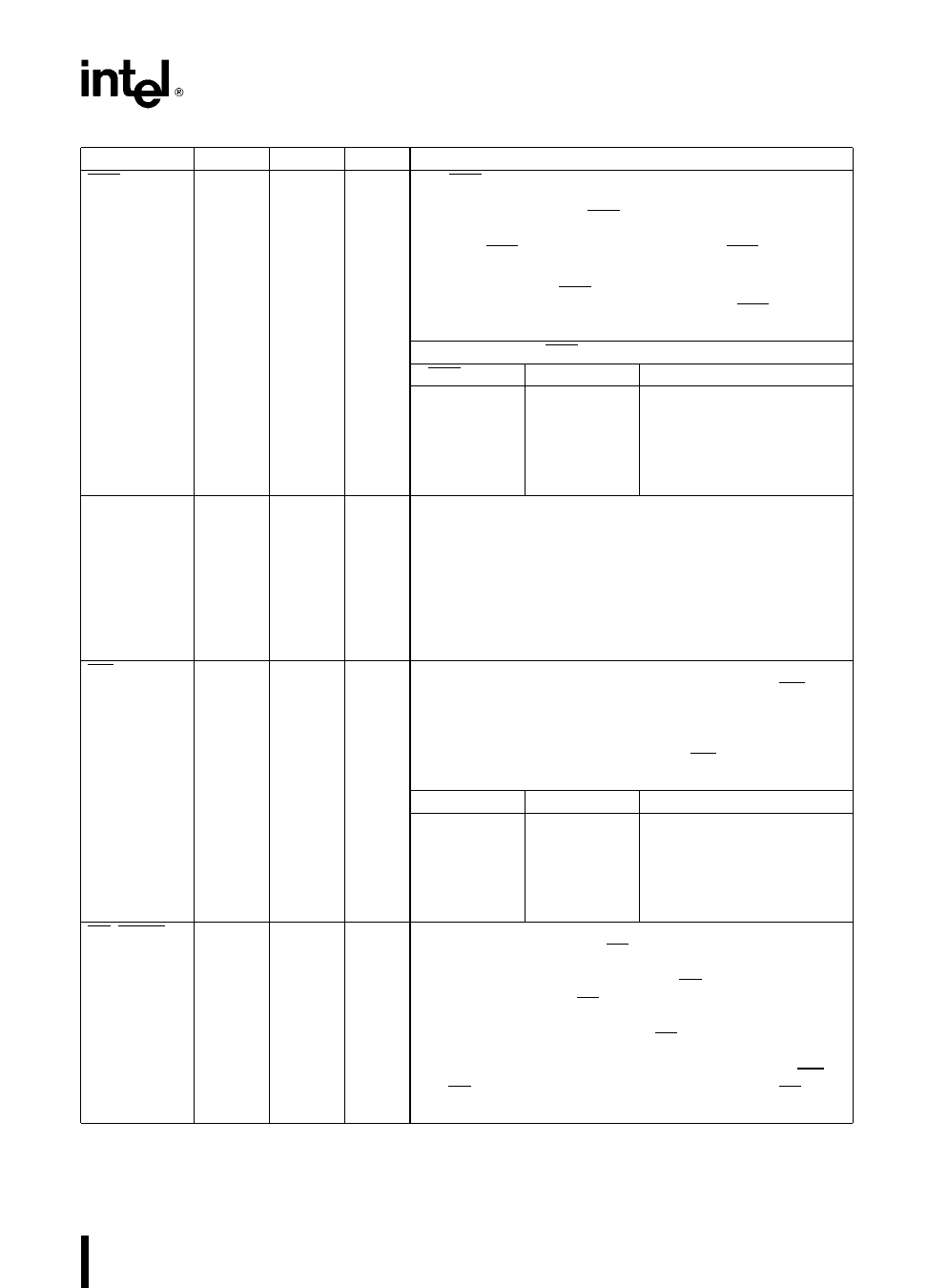
Symbol
BHE
ALE QS0
WR QS1
RD QSMD
M80C186
PGA
64
61
63
62
Table 1 M80C186 Pin Description (Continued)
QFP
14
17
15
16
Type
O
O
O
O
Name and Function
The BHE (Bus High Enable) signal is analogous to A0 in that
it is used to enable data on to the most significant half of the
data bus pins D15 – D8 BHE will be LOW during T1 when the
upper byte is transferred and will remain LOW through T3
AND TW BHE does not need to be latched BHE will float
during HOLD
In Enhanced Mode BHE will also be used to signify DRAM
refresh cycles A refresh cycle is indicated by BHE and A0
being HIGH
BHE and A0 Encodings
BHE Value
A0 Value
Function
0
0
Word Transfer
0
1
Byte Transfer on upper half
of data bus (D15 – D8)
1
0
Byte Transfer on lower half
of data bus (D7 – D0)
1
1
Refresh
Address Latch Enable Queue Status 0 is provided by the
M80C186 to latch the address ALE is active HIGH
Addresses are guaranteed to be valid on the trailing edge of
ALE The ALE rising edge is generated off the rising edge of
the CLKOUT immediately preceding T1 of the associated bus
cycle effectively one-half clock cycle earlier than in the
standard M8086 The trailing edge is generated off the
CLKOUT rising edge in T1 as in the M8086 Note that ALE is
never floated
Write Strobe Queue Status 1 indicates that the data on the
bus is to be written into a memory or an I O device WR is
active for T2 T3 and TW of any write cycle It is active LOW
and floats during ‘‘HOLD ’’ It is driven HIGH for one clock
during Reset and then floated When the M80C186 is in
queue status mode the ALE QS0 and WR QS1 pins provide
information about processor instruction queue interaction
QS1
QS0
Queue Operation
0
0
No queue operation
0
1
First opcode byte fetched
from the queue
1
1
Subsequent byte fetched
from the queue
1
0
Empty the queue
Read Strobe indicates that the M80C186 is performing a
memory or I O read cycle RD is active LOW for T2 T3 and
TW of any read cycle It is guaranteed not to go LOW in T2
until after the Address Bus is floated RD is active LOW and
floats during ‘‘HOLD’’ RD is driven HIGH for one clock
during Reset and then the output driver is floated A weak
internal pull-up mechanism of the RD line holds it HIGH when
the line is not driven During RESET the pin is sampled to
determine whether the M80C186 should provide ALE WR
and RD or if the Queue-Status should be provided RD
should be connected to GND to provide Queue-Status data
5
Share Link: 