M80C186 データシートの表示(PDF) - Intel
部品番号
コンポーネント説明
メーカー
M80C186 Datasheet PDF : 59 Pages
| |||
M80C186
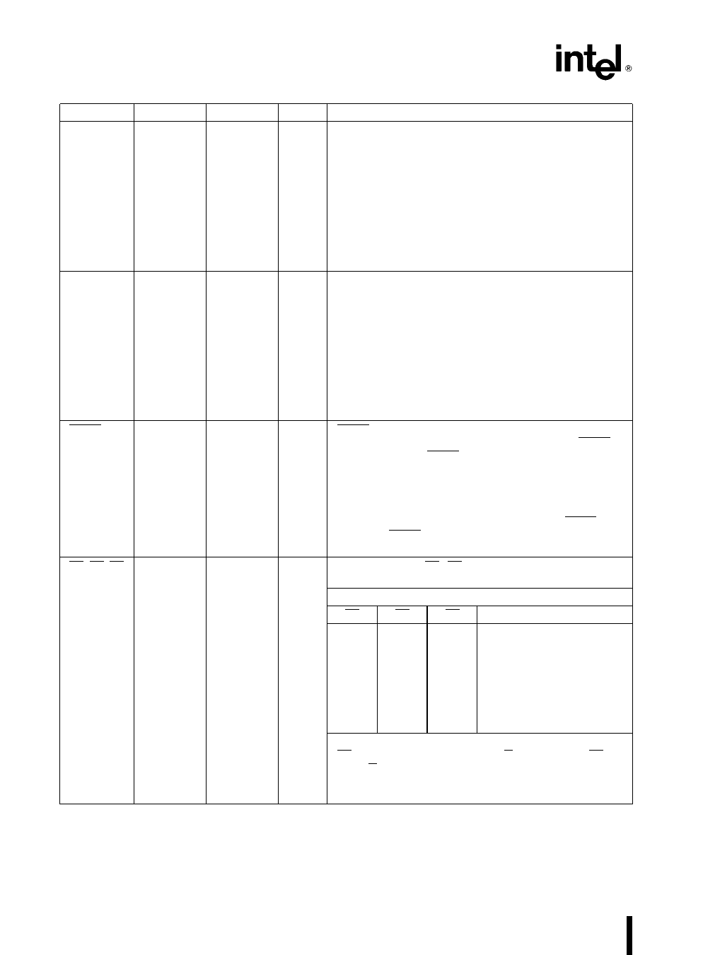
Symbol
ARDY
SRDY
LOCK
S0 S1 S2
PGA
55
49
48
52 53 54
Table 1 M80C186 Pin Description (Continued)
QFP
23
29
30
26 25 24
Type
I
I
O
O
Name and Function
Asynchronous Ready informs the M80C186 that the
addressed memory space or I O device will complete
a data transfer The ARDY input pin will accept an
asynchronous input and is active HIGH Only the rising
edge is internally synchronized by the M80C186 This
means that the falling edge of ARDY must be
synchronized to the M80C186 clock If connected to
VCC no WAIT states are inserted Asynchronous ready
(ARDY) or synchronous ready (SRDY) must be active
to terminate a bus cycle If unused this line should be
tied LOW to yield control to the SRDY pin
Synchronous Ready must be synchronized externally
to the M80C186 The use of SRDY provides a relaxed
system-timing specification on the Ready input This is
accomplished by eliminating the one-half clock cycle
which is required for internally resolving the signal level
when using the ARDY input This line is active HIGH If
this line is connected to VCC no WAIT states are
inserted Asynchronous ready (ARDY) or synchronous
ready (SRDY) must be active before a bus cycle is
terminated If unused this line should be tied LOW to
yield control to the ARDY pin
LOCK output indicates that other system bus masters
are not to gain control of the system bus while LOCK is
active LOW The LOCK signal is requested by the
LOCK prefix instruction and is activated at the
beginning of the first data cycle associated with the
instruction following the LOCK prefix It remains active
until the completion of the instruction following the
LOCK prefix No prefetches will occur while LOCK is
asserted LOCK is active LOW is driven HIGH for one
clock during RESET and then floated
Bus cycle status S0 –S2 are encoded to provide bus-
transaction information
M80C186 Bus Cycle Status Information
S2
S1
S0
Bus Cycle Initiated
0
0
0
Interrupt Acknowledge
0
0
1
Read I O
0
1
0
Write I O
0
1
1
Halt
1
0
0
Instruction Fetch
1
0
1
Read Data from Memory
1
1
0
Write Data to Memory
1
1
1
Passive (no bus cycle)
The status pins float during HOLD HLDA
S2 may be used as a logical M IO indicator and S1 as
a DT R indicator
The status lines are driven HIGH for one clock during
Reset and then floated until a bus cycle begins
6
Share Link: 