M80C186 データシートの表示(PDF) - Intel
部品番号
コンポーネント説明
メーカー
M80C186 Datasheet PDF : 59 Pages
| |||
M80C186
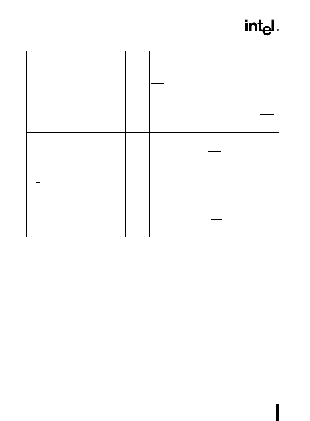
Symbol
PCS0
PCS1–4
PCS5 A1
PCS6 A2
DT R
DEN
Table 1 M80C186 Pin Description (Continued)
PGA
QFP
25
53
27 28 29 30 51 50 49 48
31
47
32
46
40
38
39
39
Type
O
O
O
O
O
O
Name and Function
Peripheral Chip Select signals 0 – 4 are active LOW
when a reference is made to the defined peripheral
area (64K byte I O space) These lines are not floated
during bus HOLD The address ranges activating
PCS0 – 4 are software programmable
Peripheral Chip Select 5 or Latched A1 may be
programmed to provide a sixth peripheral chip select or
to provide an internally latched A1 signal The address
range activating PCS5 is software programmable When
programmed to provide latched A1 rather than PCS5
this pin will retain the previously latched value of A1
during a bus HOLD A1 is active HIGH
Peripheral Chip Select 6 or Latched A2 may be
programmed to provide a seventh peripheral chip
select or to provide an internally latched A2 signal The
address range activating PCS6 is software
programmable When programmed to provide latched
A2 rather than PCS6 this pin will retain the previously
latched value of A2 during a bus HOLD A2 is active
HIGH
Data Transmit Receive controls the direction of data
flow through the external M8286 M8287 data bus
transceiver When LOW data is transferred to the
M80C186 When HIGH the M80C186 places write data
on the data bus
Data Enable is provided as an M8286 M8287 data bus
transceiver output enable DEN is active LOW during
each memory and I O access DEN is HIGH whenever
DT R changes state
8
Share Link: 