87L54 データシートの表示(PDF) - Intel
部品番号
コンポーネント説明
メーカー
87L54 Datasheet PDF : 20 Pages
| |||
8XL52 54 58
ALE Address Latch Enable output pulse for latching
the low byte of the address during accesses to ex-
ternal memory This pin (ALE PROG) is also the
program pulse input during OTP ROM programming
for the 87L5X
In normal operation ALE is emitted at a constant
rate of the oscillator frequency and may be used
for external timing or clocking purposes Note how-
ever that one ALE pulse is skipped during each ac-
cess to external Data Memory
If desired ALE operation can be disabled by setting
bit 0 of SFR location 8EH With this bit set the pin is
weakly pulled high However the ALE disable fea-
ture will be suspended during a MOVX or MOVC in-
struction idle mode power down mode and ICE
mode The ALE disable feature will be terminated by
reset When the ALE disable feature is suspended or
terminated the ALE pin will no longer be pulled up
weakly Setting the ALE-disable bit has no affect if
the microcontroller is in external execution mode
Throughout the remainder of this data sheet ALE
will refer to the signal coming out of the ALE PROG
pin and the pin will be referred to as the ALE PROG
pin
PSEN Program Store Enable is the read strobe to
external Program Memory
When the 8XL5X is executing code from external
Program Memory PSEN is activated twice each ma-
chine cycle except that two PSEN activations are
skipped during each access to external Data Memo-
ry
EA VPP External Access enable EA must be
strapped to VSS in order to enable the device to
fetch code from external Program Memory locations
0000H to 0FFFH Note however that if either of the
Program Lock bits are programmed EA will be inter-
nally latched on reset
EA must be strapped to VCC for internal program
executions
This pin also receives the programming supply volt-
age (VPP) during OTP ROM programming
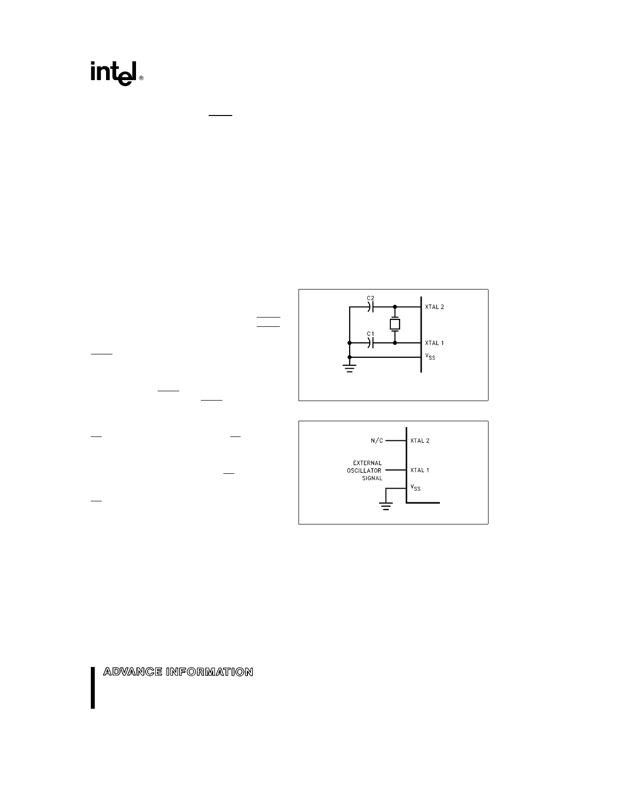
XTAL1 Input to the inverting oscillator amplifier
XTAL2 Output from the inverting oscillator amplifier
OSCILLATOR CHARACTERISTICS
XTAL1 and XTAL2 are the input and output respec-
tively of a inverting amplifier which can be config-
ured for use as an on-chip oscillator as shown in
Figure 3 Either a quartz crystal or ceramic resonator
may be used More detailed information concerning
the use of the on-chip oscillator is available in Appli-
cation Note AP-155 ‘‘Oscillators for Microcontrol-
lers ’’
To drive the device from an external clock source
XTAL1 should be driven while XTAL2 floats as
shown in Figure 4 There are no requirements on the
duty cycle of the external clock signal since the in-
put to the internal clocking circuitry is through a di-
vide-by-two flip-flop but minimum and maximum
high and low times specified on the data sheet must
be observed
An external oscillator may encounter as much as a
100 pF load at XTAL1 when it starts up This is due
to interaction between the amplifier and its feedback
capacitance Once the external signal meets the VIL
and VIH specifications the capacitance will not ex-
ceed 20 pF
272468 – 4
C1 C2 e 30 pF g10 pF for Crystals
For Ceramic Resonators contact resonator manufacturer
Figure 3 Oscillator Connections
272468 – 5
Figure 4 External Clock Drive Configuration
IDLE MODE
The user’s software can invoke the Idle Mode When
the microcontroller is in this mode power consump-
tion is reduced The Special Function Registers and
the onboard RAM retain their values during Idle but
the processor stops executing instructions Idle
Mode will be exited if the chip is reset or if an en-
abled interrupt occurs The PCA timer counter can
optionally be left running or paused during Idle
Mode
5
Share Link: 