935261222557 データシートの表示(PDF) - Philips Electronics
部品番号
コンポーネント説明
メーカー
935261222557 Datasheet PDF : 36 Pages
| |||
Philips Semiconductors
ATSC 8-VSB demodulator and decoder
Preliminary specification
TDA8960
FUNCTIONAL DESCRIPTION
The internal architecture of the TDA8960 consists of
basically two parts:
• The front-end containing the AGC, carrier recovery, half
Nyquist filter, symbol timing recovery, sync recovery and
adaptive equalization
• The back-end containing the trellis decoder,
de-interleaver, the Reed Solomon decoder and
de-randomizer.
AGC
This block controls an analog gain over a range of up to
±20 dB.
The data from the A/D converter (Philips Semiconductors’
TDA8763 is recommended) arrives at the VSB
demodulator via inputs ADIN9 to ADIN0, which is10-bit
wide. The format of the incoming samples can be
programmed using the I2C-bus accessible register 08H.
By writing to bit 3 the format can be either twos
complement or binary.
The absolute value of the input signal is averaged over
several samples. The filtered signal is compared to a
threshold. The threshold consist of a 4-bit signed value
which can be programmed using the I2C-bus. The 3-state
output signal charges or discharges an off-chip ideal
integrator and is used to control the gain controller of the
tuner front-end module. The values of the signal are shown
in Table 1.
Table 1 AGC output
PIN AGCOUT
COMMENT
1
output of the filter is smaller than the
threshold
0
output of the filter is larger than the
threshold
Z
output of the filter is equal to the
threshold
The analog low-pass filter or integrator circuit should be
designed with an 8 ms time constant. The response of the
gain amplifier is linear with respect to the control voltage
over the desired range of operation.
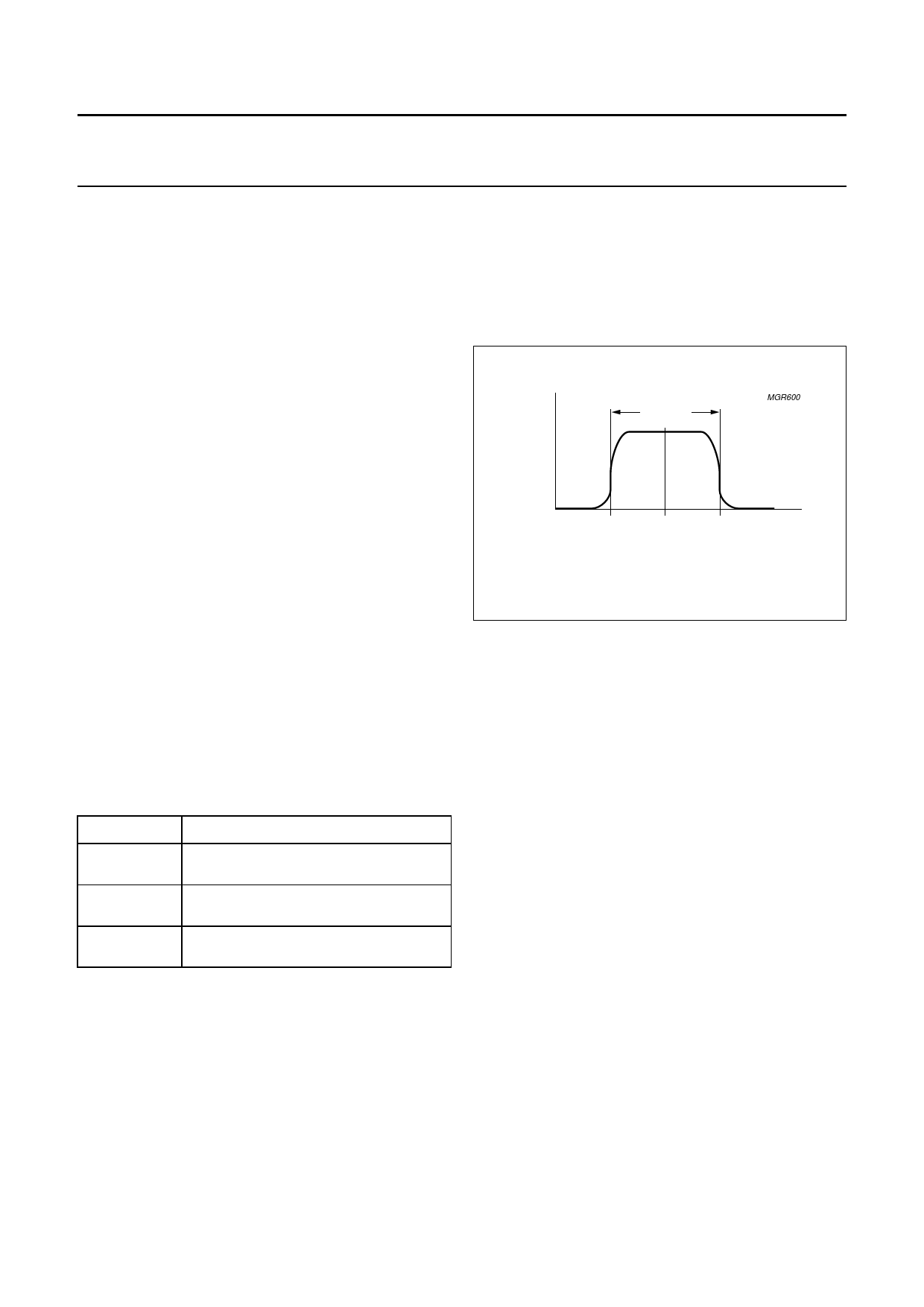
Carrier recovery
This circuit recovers the frequency and phase of the pilot
carrier. The spectrum during the carrier recovery is
displayed in Fig.3.
By default the carrier is present at 2.69 MHz. During carrier
recovery a shift is applied such that the pilot is present at
DC. It can happen that the pilot is present at the higher
edge of the VSB spectrum. In this event the CR_INV bit in
I2C-bus register 08H (see Table 13) can be set to make
sure that after the shift the pilot is at DC.
handbook, halfpage
amplitude
(dB)
5.38 MHz
MGR600
2.69
5.38
8.07
frequency (MHz)
Fig.3 Signal spectrum during carrier recovery.
The carrier recovery is capable of tracking a frequency
offset of up to 100 kHz from the nominal frequency offset
within 100 ms.
By means of I2C-bus read register 03H the current
frequency offset in the carrier recovery can be read.
This value can be used for fine tuning applications.
Sync recovery and pilot removal
This block performs several functions including pilot
removal, segment and field sync removal and rescale
AGC based on the segment sync. If this block is able to
find a data segment sync signal, the external pin
LOCKINDIC is asserted. The value of this signal can also
be read through I2C-bus control.
Adaptive equalization
The equalizer consists of a forward filter and a feedback
filter section. Demodulated symbols from the
synchronization and pilot removal block are received every
symbol period. The equalizer tries to invert the effects of
the channel on the transmitted symbol stream by filtering
these symbols. The coefficients of the filters are updated
every symbol period using the training sequence. There is
also a provision to perform blind equalization. The filtered
output is available for the next block, the trellis decoder.
1999 Jun 14
9
Share Link: 