TDK5110 データシートの表示(PDF) - Infineon Technologies
部品番号
コンポーネント説明
メーカー
TDK5110 Datasheet PDF : 41 Pages
| |||
TDK 5110
Functional Description
4
LF
VS
140 pF
15 pF
35 kΩ
10 kΩ
4
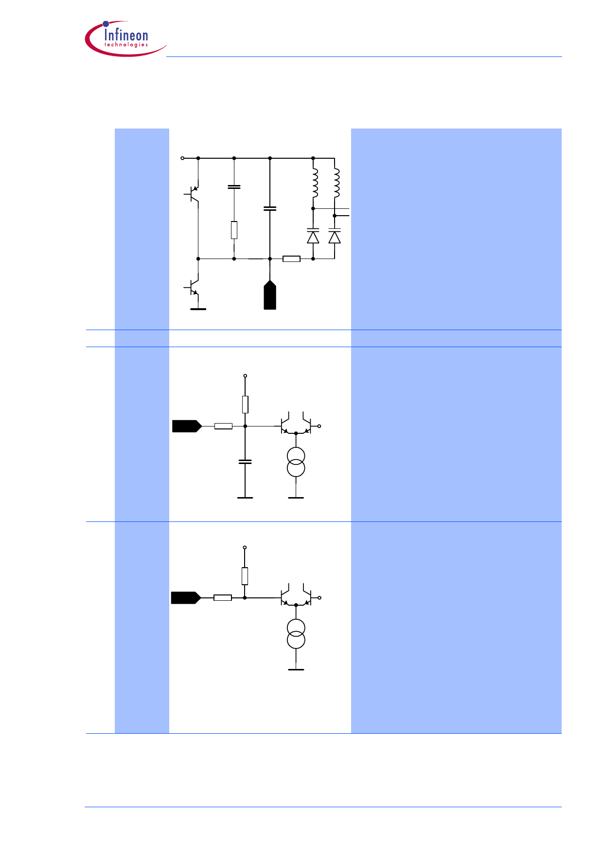
Output of the charge pump and input of the
VCO control voltage.
The loop bandwidth of the PLL is 150 kHz
when only the internal loop filter is used.
The loop bandwidth may be reduced by
applying an external RC network referencing
to the positive supply VS (pin 3).
5
GND
6 ASKDTA
+1.2 V
60 kΩ
6
90 kΩ
50 pF
General ground connection.
Digital amplitude modulation can be
imparted to the Power Amplifier through this
pin.
A logic high (ASKDTA > 1.5 V or open)
enables the Power Amplifier.
+1.1 V
30 µA
A logic low (ASKDTA < 0.5 V)
disables the Power Amplifier.
7 FSKDTA
+1.2 V
60 kΩ
7
90 kΩ
Digital frequency modulation can be
imparted to the Xtal Oscillator by this pin.
The VCO-frequency varies in accordance to
the frequency of the reference oscillator.
A logic high (FSKDTA > 1.5V or open)
+1.1 V sets the FSK switch to a high impedance
state.
30 µA
A logic low (FSKDTA < 0.5 V)
closes the FSK switch
from FSKOUT (pin 11) to FSKGND (pin 12).
A capacitor can be switched to the reference
crystal network this way. The Xtal Oscillator
frequency will be shifted giving the designed
FSK frequency deviation.
Wireless Components
3-4
Specification, October 2002
Share Link: 