TEA0678 データシートの表示(PDF) - Philips Electronics
部品番号
コンポーネント説明
メーカー
TEA0678
Philips Electronics

TEA0678 Datasheet PDF : 28 Pages
| |||
Philips Semiconductors
Dual Dolby* B-type noise reduction circuit, automatic
music search, with differential outputs and mute
Preliminary specification
TEA0678
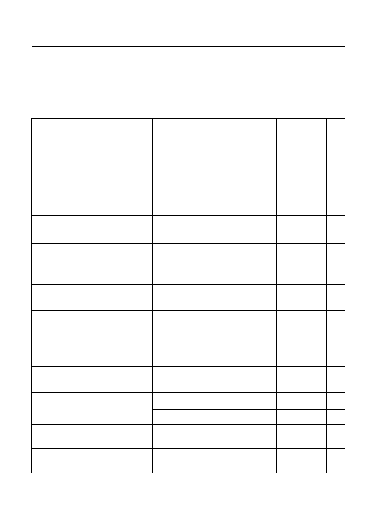
CHARACTERISTICS
VCC = 10 V; f = 20 Hz to 20 kHz; Tamb = 25 °C; nominal load 10 kΩ; all levels are referenced to 775 mV (RMS) (0 dB) at
differential outputs (Vo = Vo+ − Vo−), this corresponds to Dolby level 387.5 mV (RMS) (0 dB) at test point (OUTC);
see Fig.1; NR on/AMS off; EQ switch in the 70 µs position; unless otherwise specified.
SYMBOL
PARAMETER
CONDITIONS
MIN. TYP. MAX. UNIT
VCC
ICC
αm
Gv
Gmm
THD
HR
S------N+-----N---
Vno(rms)
PSRR
fo
αcs
αcc
RL
CL
Gv
supply voltage
7.6
supply current
channel matching
pins 14, 16, 17 and 19 connected to −
Vref
f = 1 kHz; Vo = 0 dB at each output −
f = 1 kHz; Vo = 0 dB; NR off;
−0.5
OUTA/OUTB
voltage gain (output stage)
between OUT and OUTC; f = 1 kHz; 5.5
NR off
voltage gain mismatch
(output stage)
mismatch between OUT+ and
−0.5
OUT−; f = 1 kHz; NR off
total harmonic distortion (2nd f = 1 kHz; Vo = 0 dB
−
and 3rd harmonic)
f = 10 kHz; Vo = 6 dB
−
headroom at output
signal plus noise-to-noise
ratio
VCC = 9 V; THD = 1%; f = 1 kHz
13
internal gain 40 dB; linear;
78
CCIR/ARM weighted; decode mode;
see Fig.10
equivalent input noise voltage NR off; unweighted;
−
in decode mode (RMS value) f = 20 Hz to 20 kHz; Rsource = 0 Ω
power supply ripple rejection Vi(rms) = 0.25 V; f = 1 kHz; see Fig.7 52
for unsymmetrical signal at OUTC
at differential OUT; note 1
49
frequency response
measured in encode mode;
referenced to TP
channel separation
crosstalk between active and
inactive input
see Fig.10
Vo = −25 dB; f = 0.2 kHz
Vo = 0 dB; f = 1 kHz
Vo = −25 dB; f = 1 kHz
Vo = −25 dB; f = 5 kHz
Vo = −35 dB; f = 10 kHz
Vo = +10 dB; f = 1 kHz; see Fig.8
NR off; f = 1 kHz; Vo = +10 dB;
see Fig.8
−22.9
−1.5
−17.8
−18.1
−24.4
61
70
load resistance at each output AC-coupled f = 1 kHz; Vo = 12 dB; 10
OUTA+, OUTA−, OUTB+ and THD = 1%
OUTB− (corresponds to 2 kΩ THD = 1%; note 2
1
at differential output)
capacitive load at each output CLmin at each output to ground
0.3
(between OUT+ and OUT−) (pins 1, 2, 31 and 32)
and ground
voltage gain of pre-amplifier
from pin INA1 or INA2 to pin EQFA 29
and from pin INB1 or INB2 to
pin EQFB; f = 1 kHz
10
25
26
−
6
−
0.08
0.15
−
84
−
57
52
−24.4
0
−19.3
−19.6
−25.9
67
77
−
−
−
30
12 V
28 mA
37 mA
+0.5 dB
6.5 dB
+0.5 dB
0.15 %
0.3 %
−
dB
−
dB
1.4 µV
−
dB
−
dB
−25.9 dB
+1.5 dB
−20.8 dB
−21.1 dB
−27.4 dB
−
dB
−
dB
−
kΩ
−
kΩ
1.3 nF
31 dB
1996 Jun 06
6
Share Link: