TK15400 データシートの表示(PDF) - Toko America Inc
部品番号
コンポーネント説明
メーカー
TK15400 Datasheet PDF : 12 Pages
| |||
TK15400
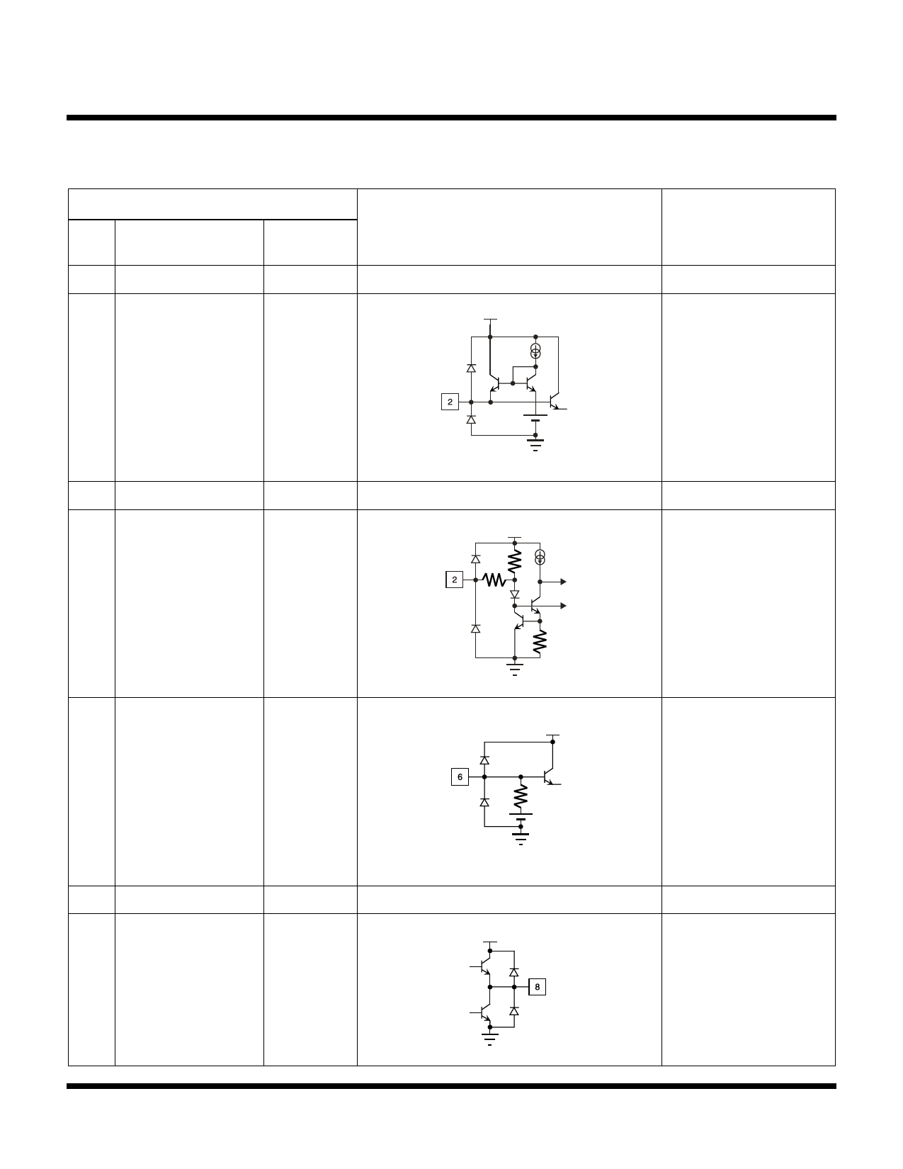
PIN FUNCTION DESCRIPTION
TERMINAL
PIN
NO.
SYMBOL
VOLTAGE
INTERNAL EQUIVALENT CIRCUIT
DESCRIPTION
1
VCC
VCC
2
Y-INPUT
1.25 V
VCC
Power supply terminal
Pin 2 is the Y signal
input terminal.
The clamp circuit fixes
the synchronous
voltage to 1.25 V.
1.25 V
3,4
GND
5
STANDBY
GND
1.4 V
6
C-INPUT
2.0 V
VCC
200 k
5k
VCC
100 k
2.0 V
GND terminal
Pin 5 is the standby
logic terminal.
The device is in the
active state when Pin 5
is pulled up to high level
or open.
The device is in the
standby state when Pin
5 is pulled down to low
level.
Pin 6 is the C signal
input terminal.
The bias circuit fixes the
C signal to 2.0 V by the
100 kΩ bias resistor.
7
GND
GND
8
C-OUTPUT
2.0 V
VCC
GND terminal
Pin 8 is the C signal
output terminal.
Pin 8 is available to
drive a 75 Ω + 75 Ω
load.
Page 8
January 2000 TOKO, Inc.
Share Link: 