TK65015MBX データシートの表示(PDF) - Toko America Inc
部品番号
コンポーネント説明
メーカー
TK65015MBX Datasheet PDF : 8 Pages
| |||
TK65015
ABSOLUTE MAXIMUM RATINGS
All pins except GND ................................................... 6 V
Power Dissipation (Note1) ................................. 400 mW
Storage Temperature Range ................... -55 to +150 °C
Operating Temp. Range ............................-10 to + 50 °C
Lead Soldering Temperature (10 s) ...................... 240 °C
Junction Temperature ........................................... 150 °C
ELECTRICAL CHARACTERISTICS
Over operating temperature range, unless otherwise specified.
VARIABLE
PARAMETER
TEST CONDITION
MIN TYP MAX UNIT
VIN
Supply Voltage range
0.90
1.60 V
VUVL
Undervoltage lockout threshold
TA = 25 °C
.74
V
I (VIN)
Quiescent current into VIN pin
VIN = 1.3 V
20
35
µA
I (VOUT)
Quiescent current into VOUT pin
VOUT = VOUT (REG) +20 mV
22
34
µA
ƒ(OSC)
Internal oscillator frequency
VIN = 0.9 V & VIN = 1.6 V 70
83 102 kHz
Temperature stability of oscillator
VIN = 1.3 V
800
ppm/°C
D(OSC)
On-time duty ratio of oscillator
VIN = 0.9V & VIN = 1.6 V
36
50
64
%
VOUT(REG) Regulation threshold of VOUT
VIN = 0.9 V & VIN = 1.6 V 2.85 3.00
3.10 V
Temperature stability of VOUT(REG)
VIN = 1.3 V
250
ppm/°C
∆VOUT(LINE) Line regulation of VOUT(REG)
VIN = 0.9 V & VIN = 1.6 V -20
0
20 mV
∆VO (LOAD) Load regulation of VOUT(REG) (Note 2) 0mA < IO < 4mA
0
mV
VOUT(RST) VOUT during reset transition
2.48
2.70 V
∆VOUT(RST) VOUT(RST) threshold hysteresis
45
mV
VRST(HI)
Logic High of RESET w/r/t VOUT
300 kΩ Pullup
-100
mV
VRST(LO)
Logic Low of RESET
300 kΩ Pullup
100 mV
RSW(ON)
On-resistance of switch, IND pin
VOUT = VOUT(REG)
0.5
ohms
0
II(Q)
Quiescent current of converter (Note 5) VI = 1.3 V, IO = 0mA
80
120 µA
IO(MAX)
Maximum IO for converter (Notes 3,5) VI ≥ 1.1 V, VO Regulated
4
mA
η
Converter efficiency (Notes 4,5)
VI = 1.3 V, IO = 4 mA
74
%
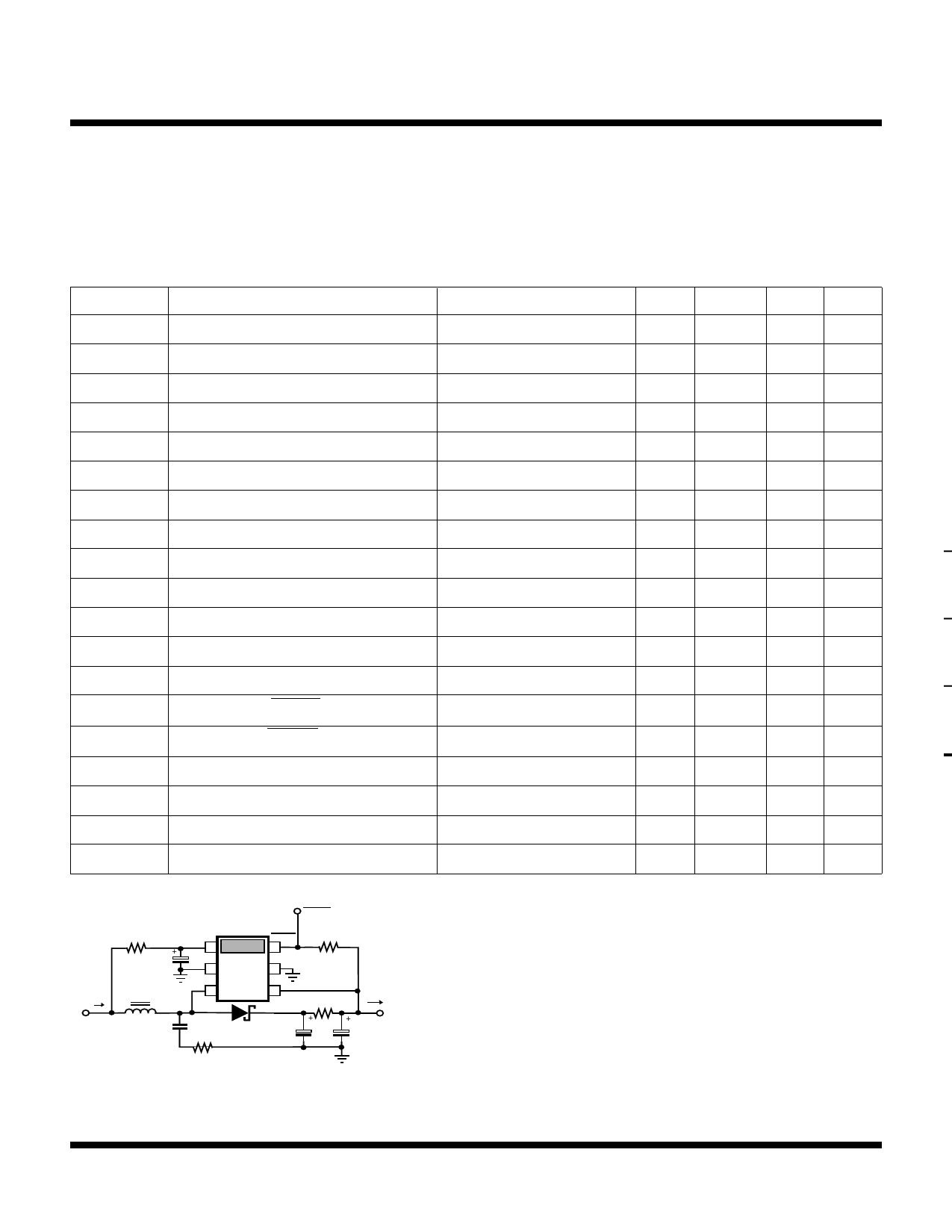
TEST CIRCUIT
II
VI
1K
CS
10 µF
L = 95 µH
220 pF
VIN
1
GND
2
IND
3
D
1K
RESET
RESET
6
GND
5
VOUT
4
C1
10 µF
300 kΩ
15
IO
VO
C2
10 µF
Inductor L: Toko A682AE-014=P3 or equivalent
Diode D: LL103A or equivalent
Note 1: Derate at 0.8 mW/oC for operation above TA = 25 oC ambient tempera-
ture, when heat conducting copper foil path is maximized on the printed circuit
board. When this is not possible, a derating factor of 1.6 mW/ °C must be used.
Note 2: The output regulation threshold, VOUT(REG), is guaranteed-by-design to
be independent of the load. Regulation will occur provided that the load current is
within the capability of the converter, IO(MAX). The output voltage may fluctuate
slightly with load due to the variation of the ripple voltage, whose magnitude is
primarily determined by the inductor and the ESR of the output capacitors.
Note 3: Maximum load current depends on inductor value. With a 0.9 V or 1.0 V
supply voltage, 4 mA can be obtained with a smaller inductor value.
Note 4: Converter efficiency is a function of the diode forward voltage and
inductor winding resistance. It may also depend in varying degree on the inductor
value and capacitor ESRs. By trading component size for better specifications,
efficiency greater than 80% can be attained.
Note 5: Test performed using the test circuit below.
Page 2
2-2-96
February, 1996 TOKO, Inc.
Share Link: 