HT23C128 „Éá„Éľ„āŅ„ā∑„Éľ„Éą„ĀģŤ°®Á§ļÔľąPDFÔľČ - Holtek Semiconductor
ťÉ®ŚďĀÁē™ŚŹ∑
„ā≥„É≥„ÉĚ„Éľ„Éć„É≥„ÉąŤ™¨śėé
„É°„Éľ„āę„Éľ
HT23C128 Datasheet PDF : 8 Pages
| |||
HT23C128
Functional Description
The HT23C128 has two modes, namely data
read mode and standby mode, controlled by
CE/CE/OE2/OE2, OE/OE/NC and OE1/OE1/NC
inputs.
‚ÄĘ Standby mode
The HT23C128 has lower current consumption,
controlled by the chip enable input (CE/CE).
When a low/high level is applied to the CE/CEB
input regardless of the output enable
(OE/OE/NC and OE1/OE1/NC) states, the chip
will enter the standby mode.
‚ÄĘ Data read mode
When both the chip enable (CE/CE/OE2/OE2)
and the output enable (OE/OE/NC and
OE1/OE1/NC) are active, the chip is in data
read mode. Otherwise, active CE/CE and in-
active OE/OE/NC or OE1/OE1/NC result in
deselect mode. The output will remain in Hi-Z
state.
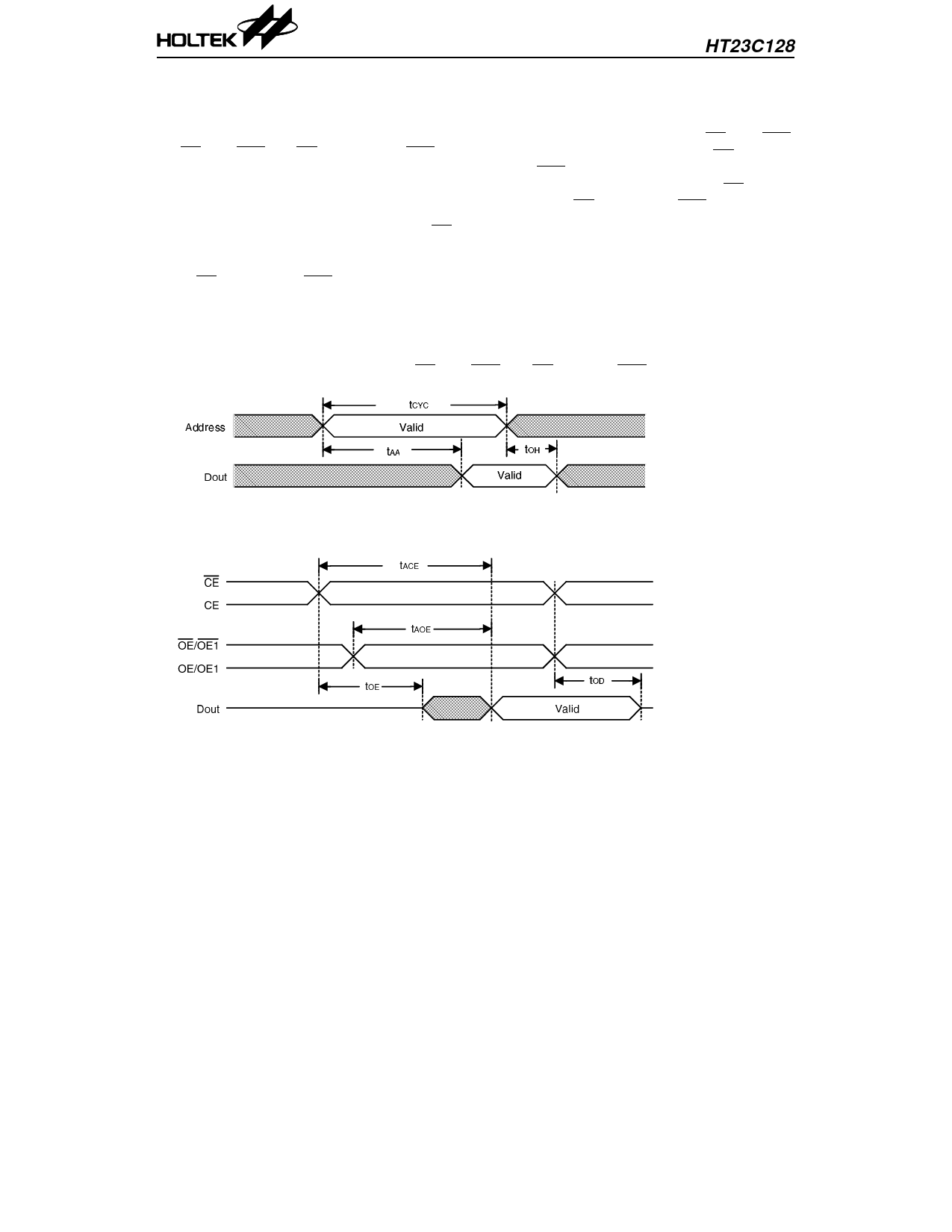
Timing Diagrams
‚ÄĘ Propagation delay due to address (CE/CE/OE2/OE2, OE/OE and OE1/OE1 are active)
‚ÄĘ Propagation delay due to chip enable and output enable (address valid)
5
24th Aug ’98
Share Link: 