HT23C040 データシートの表示(PDF) - Holtek Semiconductor
部品番号
コンポーネント説明
メーカー
HT23C040 Datasheet PDF : 10 Pages
| |||
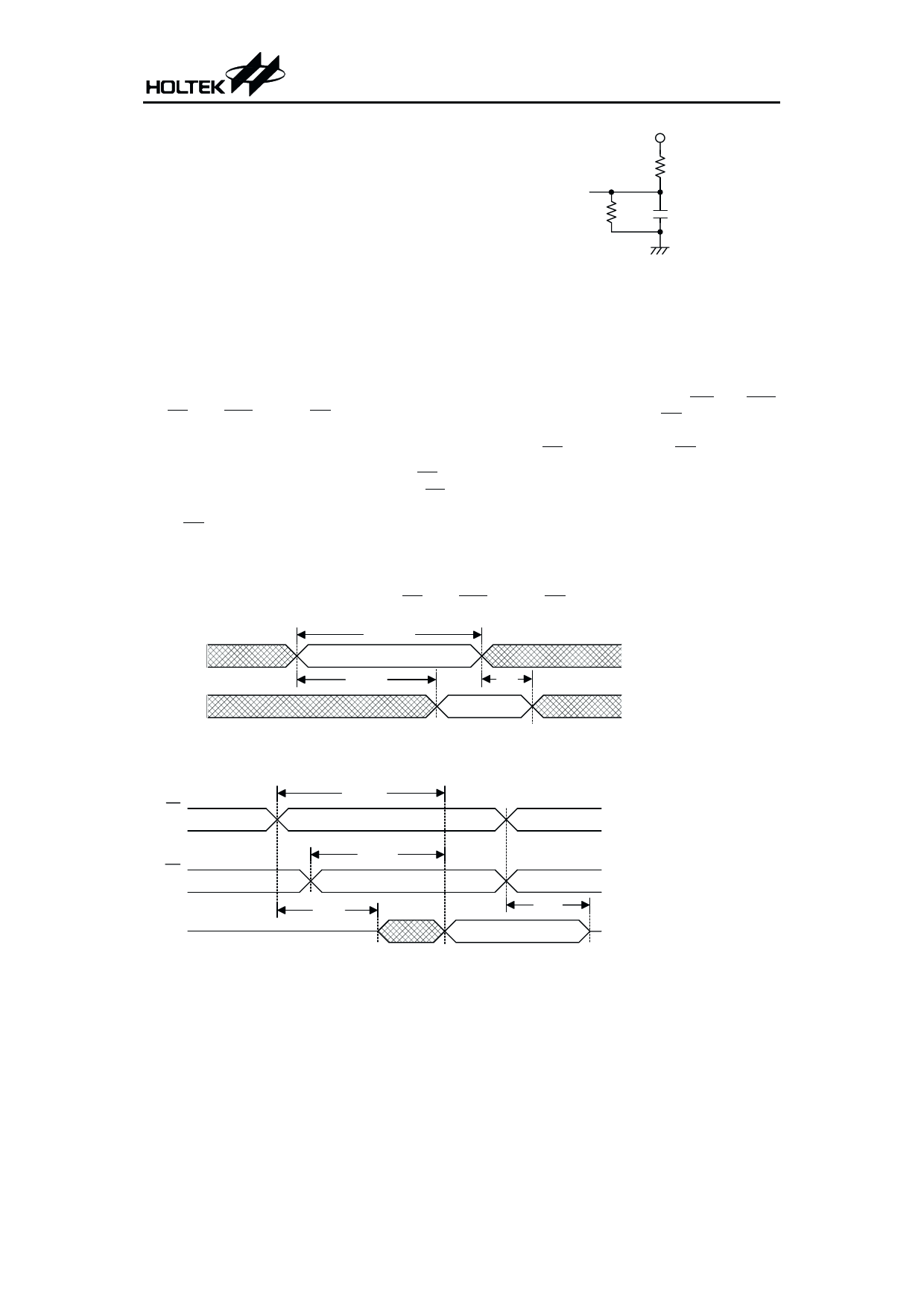
A.C. test condition
Output load: see figure right
Input rise and fall time: 10ns
Input pulse levels: 0.4V to 2.4V
Input and output timing reference levels:
0.8V and 2.0V (VCC=5V)
1.5V (VCC=3V)
O u tp u t
775W
HT23C040
V CC
1250W
100pF*
* In c lu d in g s c o p e a n d jig
Output load circuit
Functional Description
The HT23C040 has two modes, namely data
read mode and standby mode, controlled by
CE/CE/OE1/OE1 and OE/OE/NC inputs.
· Standby mode
The HT23C040 has lower current consumption,
controlled by the chip enable input (CE/CE).
When a low/high level is applied to the CE/CE
input regardless of the output enable
(OE/OE/NC) states, the chip will enter the
standby mode.
· Data read mode
When both the chip enable (CE/CE/OE1/OE1)
and the output enable (OE/OE/NC) are active,
the chip is in data read mode. Otherwise, ac-
tive CE/CE and inactive OE/OE/NC result in
deselect mode. The output will remain in Hi-Z
state.
Timing Diagrams
· Propagation delay due to address (CE/CE/OE1/OE1 and OE/OE are active)
A d d re s s
D out
tC Y C
V a lid
tA A
tO H
V a lid
· Propagation delay due to chip and output enable (address valid)
CE
CE
OE
OE
D out
tA C E
tA O E
tO E
tO D
V a lid
6
January 20, 2000
Share Link: 