MP7645B データシートの表示(PDF) - Exar Corporation
部品番号
コンポーネント説明
メーカー
MP7645B Datasheet PDF : 8 Pages
| |||
MP7645B
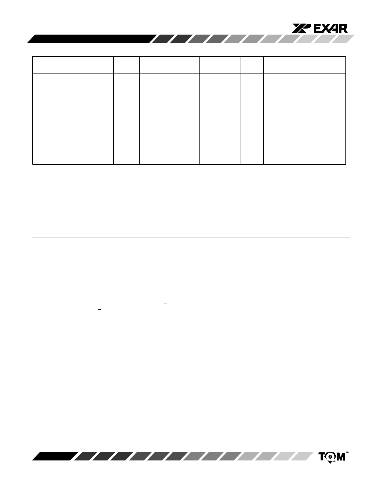
ELECTRICAL CHARACTERISTICS (CONT’D)
Parameter
25°C
Symbol Min Typ Max
POWER SUPPLY
Tmin to Tmax
Min Max Units
Test Conditions/Comments
Functional Voltage Range5
Supply Current
SWITCHING
CHARACTERISTICS2, 4
VDD
5
IDD
15
5
15 V
1
1 mA
All digital inputs = 0 V or all = 5 V
Chip Select to Write Set-Up Time
tCS
180
ns
Chip Select to Write Hold Time
tCH
0
ns
Write Pulse Width
tWR
100
ns
Data Valid to Write Set-Up Time
tDS
100
ns
Data Valid to Write Hold Time
tDH
10
ns
NOTES:
1 Full Scale Range (FSR) is 10V for unipolar mode.
2 Guaranteed but not production tested.
3 Digital input levels should not go below ground or exceed the positive supply voltage, otherwise damage may occur.
4 See timing diagram.
5 Specified values guarantee functionality. Refer to other parameters for accuracy.
Specifications are subject to change without notice
ABSOLUTE MAXIMUM RATINGS (TA = +25°C unless otherwise noted)1, 2, 3
VDD to GND . . . . . . . . . . . . . . . . . . . . . . . . . . . . . . . . . . . +17 V
Digital Input Voltage to GND (2) . GND –0.5 to VDD +0.5 V
IOUT1, IOUT2 to GND . . . . . . . . . . . GND –0.5 to VDD +0.5 V
VREF to GND (2) . . . . . . . . . . . . . . . . . . . . . . . . . . . . . . . +25 V
VRFB to GND (2) . . . . . . . . . . . . . . . . . . . . . . . . . . . . . . . +25 V
AGND to DGND . . . . . . . . . . . . . . . . . . . . . . . . . . . . . . . +0.5 V
(Functionality Guaranteed +0.5 V)
Storage Temperature . . . . . . . . . . . . . . . . . –65°C to +150°C
Lead Temperature (Soldering, 10 seconds) . . . . . . +300°C
Package Power Dissipation Rating to 75°C
CDIP, PDIP . . . . . . . . . . . . . . . . . . . . . . . . . . . . . . . 950mW
Derates above 75°C . . . . . . . . . . . . . . . . . . . . . 13mW/°C
NOTES:
1 Stresses above those listed under “Absolute Maximum Ratings” may cause permanent damage to the device. This is a
stress rating only and functional operation at or above this specification is not implied. Exposure to maximum rating
conditions for extended periods may affect device reliability.
2 Any input pin which can see a value outside the absolute maximum ratings should be protected by Schottky diode clamps
(HP5082-2835) from input pin to the supplies.
3 GND refers to AGND and DGND.
Rev. 2.00
4
Share Link: 