42754G データシートの表示(PDF) - Infineon Technologies
部品番号
コンポーネント説明
メーカー
42754G Datasheet PDF : 29 Pages
| |||
4
General Product Characteristics
TLE42754
General Product Characteristics
4.1
Absolute Maximum Ratings
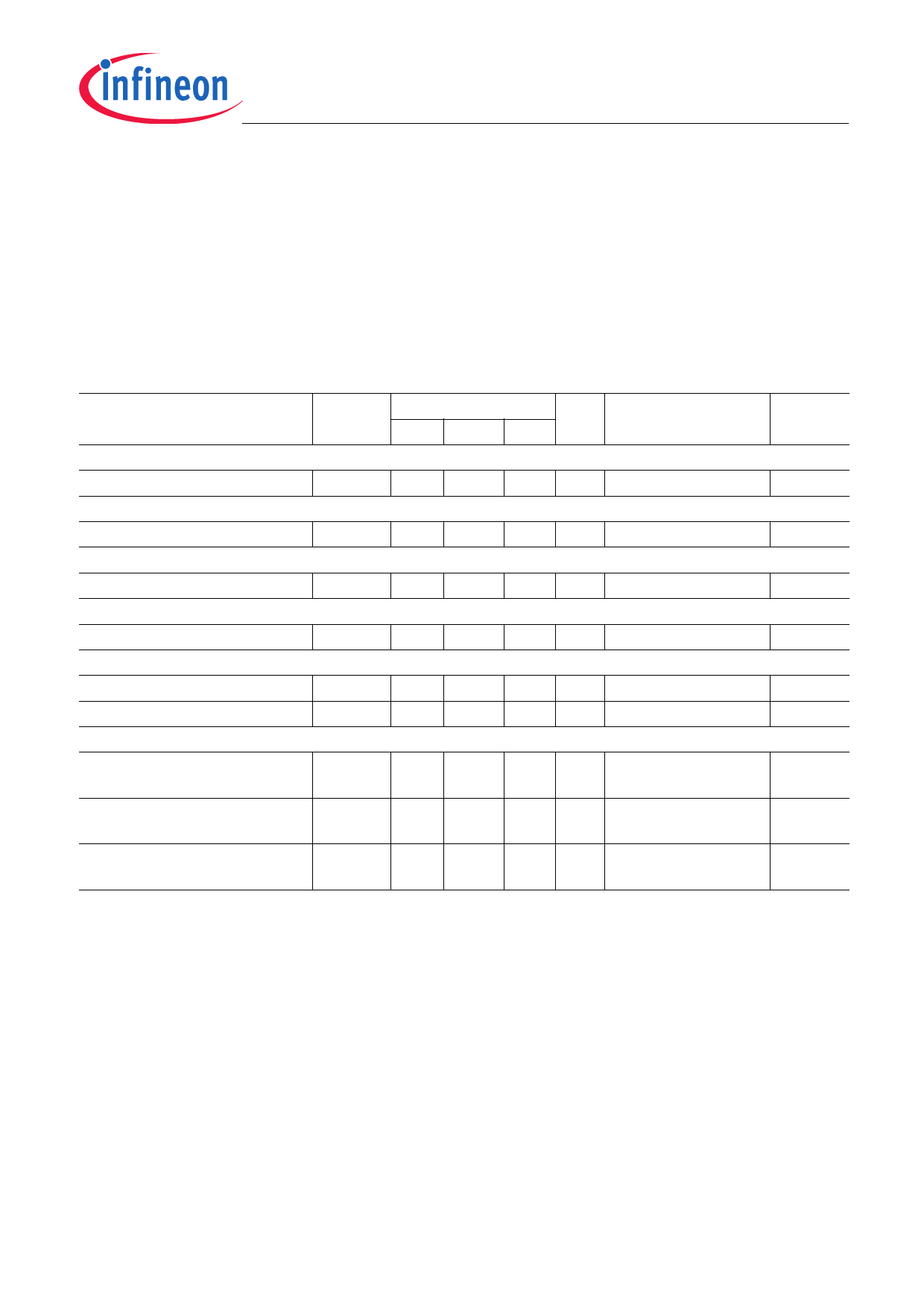
Table 1 Absolute Maximum Ratings1)
-40 °C ≤ Tj ≤ 150°C; all voltages with respect to ground, positive current flowing into pin (unless otherwise
specified)
Parameter
Symbol
Values
Unit Note / Test Condition Number
Min. Typ. Max.
Input
Voltage
Output
VI
-42 –
45 V –
P_4.1.1
Voltage
Reset Output
VQ
-0.3 –
7
V–
P_4.1.2
Voltage
Reset Delay
VRO
-0.3 –
25 V –
P_4.1.3
Voltage
Temperature
VD
-0.3 –
7
V–
P_4.1.4
Junction Temperature
Storage Temperature
ESD Absorption
Tj
-40 –
150 °C –
Tstg
-50 –
150 °C –
P_4.1.5
P_4.1.6
ESD Absorption
VESD,HBM -2
–
2
kV Human Body Model P_4.1.7
(HBM)2)
ESD Absorption
VESD,CDM -500 –
500 V
Charge Device Model P_4.1.8
(CDM)3)
ESD Absorption
VESD,CDM -750 –
1) Not subject to production test, specified by design.
2) ESD HBM Test according AEC-Q100-002 - JESD22-A114
3) ESD CDM Test according ESDA STM5.3.1
750 V
Charge Device Model P_4.1.9
(CDM)3) at corner pins
Notes
1. Stresses above the ones listed here may cause permanent damage to the device. Exposure to absolute
maximum rating conditions for extended periods may affect device reliability.
2. Integrated protection functions are designed to prevent IC destruction under fault conditions described in the
data sheet. Fault conditions are considered as “outside” normal operating range. Protection functions are not
designed for continuous repetitive operation.
Data Sheet
7
Rev. 1.2, 2014-07-03
Share Link: 