TS1582CM5(2003) データシートの表示(PDF) - TSC Corporation
部品番号
コンポーネント説明
メーカー
TS1582CM5 Datasheet PDF : 7 Pages
| |||
Application Information (continued)
The effect on output regulation can be seen in trace B
of Figure 3. It is important to note that the voltage drops
due to Rp are not eliminated; they will add to the
dropout voltage of the regulator regardless. The
TS1582 can control the voltage at the load as long as
the input-output voltage is greater than the total of the
dropout voltage of the device plus the voltage drop
across Rp
Figure 3. Remote Sensing Improves Load Regulation
Because they contain parasitic resistance and
inductance, capacitors are not ideal elements. These
parasitic elements dominate the change in output
voltage as the beginning of a transient load step
change. The ESR of the output capacitors produces
and instantaneous step in output voltage
∆V = ∆I (ESR). The ESL of the output capacitors
produces a drop proportional to the rate of change of
the output current V = L (∆I / ∆t). the output
capacitance produces a change in output voltage
proportional to the time until the regulator can respond
∆V = ∆t (∆I / C).
Figure 4. illustrates there transient effects.
Stability
The circuit design used in the TS1582 Series requires
the use of an output capacitor as part of the device
frequency compensation. The addition of 150uF
aluminum electrolytic or a 22uF solid tantalum on the
output will ensure stability for all operating conditions.
In order to meet the transient performance of the
processor larger value capacitors are needed. To limit
the high frequency noise generated by the processor
high quality bypass capacitors must be used. In order
to limit parasitic inductance (ESL) and resistance
(ESR) in capacitors to acceptable limits, multiple small
ceramic capacitors in addition to high quality solid
tantalum capacitors are required.
When the adjustment terminal is bypass to improve the
ripple rejection, the requirement for an output capacitor
increases. The Adjust pin is brought out on the fixed
voltage device specifically to allow this capability. To
further improve stability and transient response of
these devices larger values of output capacitor can be
used. The modern processors generate large high
frequency current transients. The load current step
contains higher order frequency components than the
output coupling network must handle until the regulator
throttles to the load current level.
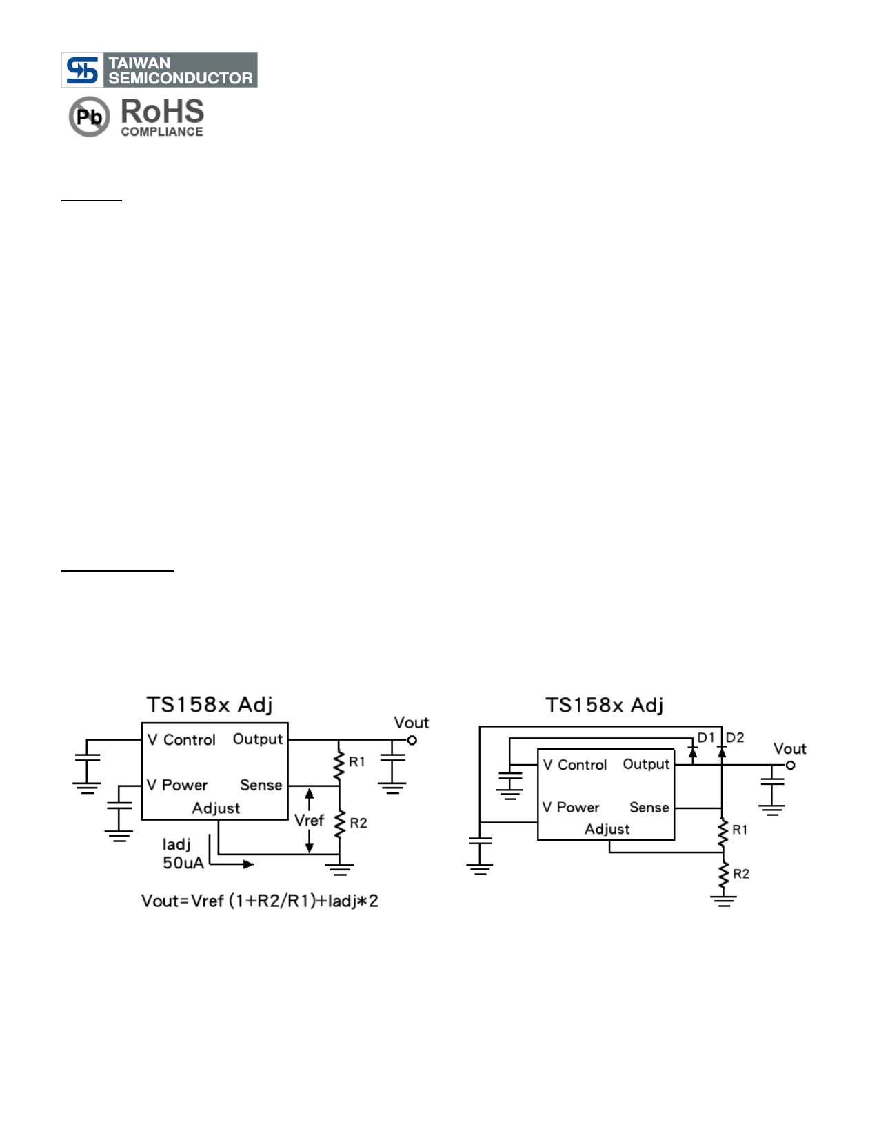
Output voltage
The TS1582 (adjustable version) develops a 1.25V
reference voltage between the Sense Pin and the
Adjust Pin (Figure 5). Placing a resistor between these
two terminals causes a constant current to flow though
R1 and down though R2 to set the output voltage. In
general R1 is chosen so that this current is the
specified minimum load current of 10mA. The current
out of the Adjust pin is small, typically 50uA and it adds
to the current from R1.For best regulation the top of the
resistor divider should be connected directly to the
Sense pin.
Figure 5. Setting Output Voltage
TS1582 series
5-5
2003/12 rev. A
Share Link: 