TSA5514 データシートの表示(PDF) - Philips Electronics
部品番号
コンポーネント説明
メーカー
TSA5514 Datasheet PDF : 18 Pages
| |||
Philips Semiconductors
1.3 GHz bidirectional I2C-bus controlled synthesizer
Product specification
TSA5514
FUNCTIONAL DESCRIPTION
The TSA5514 is controlled via the two-wire I2C-bus. For
programming, there is one module address (7 bits) and the
R/W bit for selecting READ or WRITE mode.
WRITE mode: R/W = 0 (see Table 1)
After the address transmission (first byte), data bytes can
be sent to the device. Four data bytes are required to fully
program the TSA5514. The bus transceiver has an
auto-increment facility which permits the programming of
the TSA5514 within one single transmission
(address + 4 data bytes).
The TSA5514 can also be partially programmed on the
condition that the first data byte following the address is
byte 2 or byte 4. The meaning of the bits in the data bytes
is given in Table 1. The first bit of the first data byte
transmitted indicates whether frequency data (first bit = 0)
or charge pump and port information (first bit = 1) will
follow. Until an I2C-bus STOP condition is sent by the
controller, additional data bytes can be entered without the
need to re-address the device. This allows a smooth
frequency sweep for fine tuning or AFC purpose. At
power-on the ports are set to the high impedance state.
The 7.8125 kHz reference frequency is obtained by
dividing the output of the 4 MHz crystal oscillator by 512.
Because the input of UHF/VHF signal is first divided by 8
the step size is 62.5 kHz. A 3.2 MHz crystal can offer step
sizes of 50 kHz.
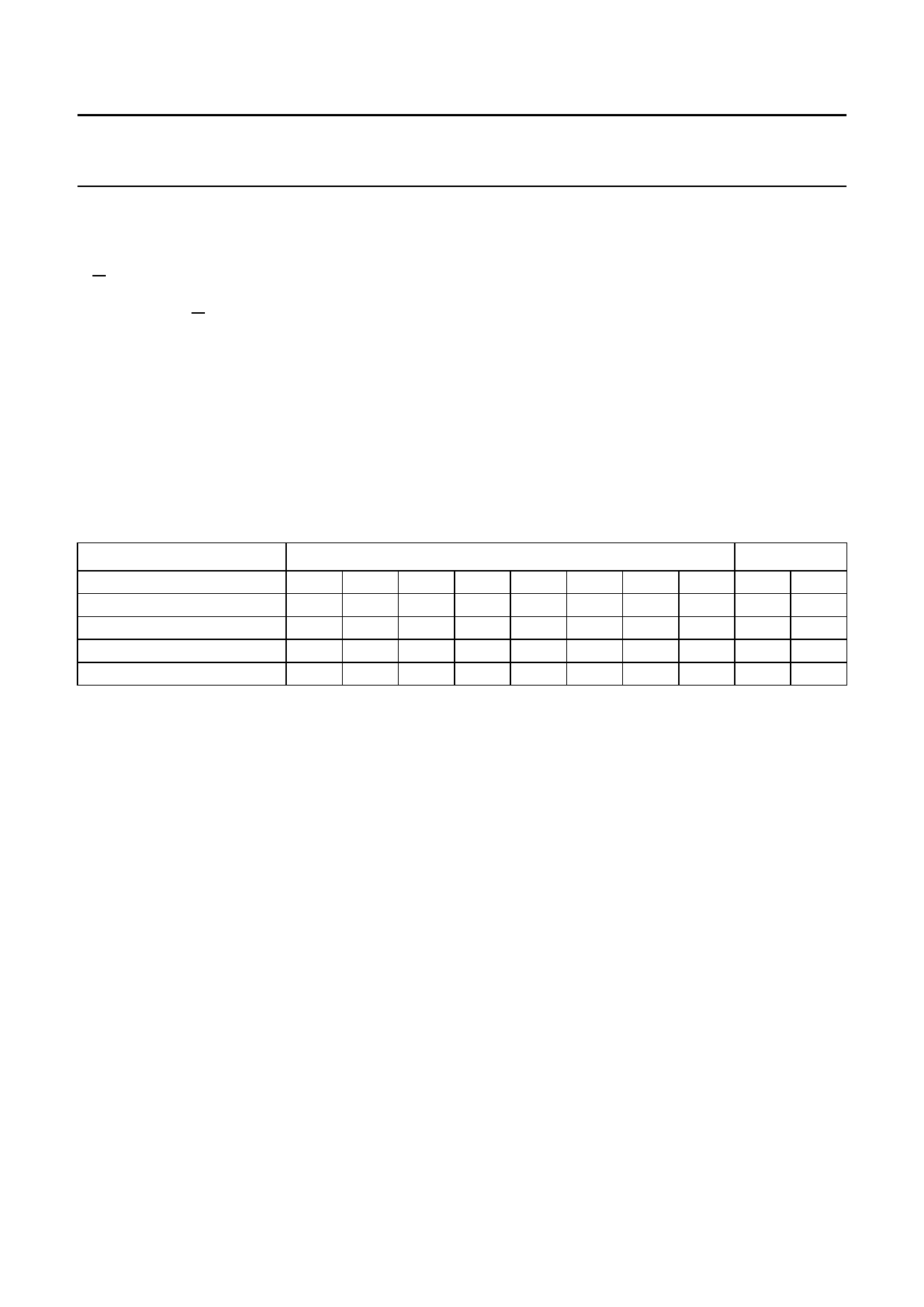
Table 1 Write data format
Address
Programmable divider
Programmable divider
Charge-pump and test bits
Output ports control bits
MSB
LSB
1
1
0
0
0 MA1 MA0 0
0
N14 N13 N12 N11 N10 N9
N8
N7 N6 N5 N4 N3 N2 N1 N0
1
CP
T1
T0
x
x
x
OS
P7
P6
P5
P4
x
P2 P1* P0*
A byte 1
A byte 2
A byte 3
A byte 4
A byte 5
Note to Table 1
*
MA1, MA0
A
N14 to N0
N = N14 × 214 + N13 × 213 +... + N1 × 21 +N0
CP
CP = 0
CP = 1
P7 to P0 = 1
P7 to P0 = 0
T1, T0, OS = 0 0 0
T1 = 1
T0 = 1
OS = 1
Not valid for TSA5514T
programmable address bits (see Table 4)
acknowledge bit
programmable divider bits
charge-pump current
50 µA
220 µA
open-collector output is active
outputs are in high impedance state
normal operation
P6 = fref, P7 = fDIV
3-state charge-pump
operational amplifier output is switched off (varicap drive disable)
Note
1. x = don’t care
October 1992
6
Share Link: 