ADM9240 データシートの表示(PDF) - Analog Devices
部品番号
コンポーネント説明
メーカー
ADM9240 Datasheet PDF : 22 Pages
| |||
The input ranges of the analog inputs are shown in more detail
in Table I.
The +VCCP1 and +VCCP2 inputs are used to measure processor
core voltages, and have an input range from 0 V to 3.6 V. If
only a single processor core voltage is being monitored, the
VCCP2 input may be used to monitor the –12 V supply. This is
achieved by using a resistive divider network referenced to a
known positive dc voltage. This is illustrated in Figure 4.
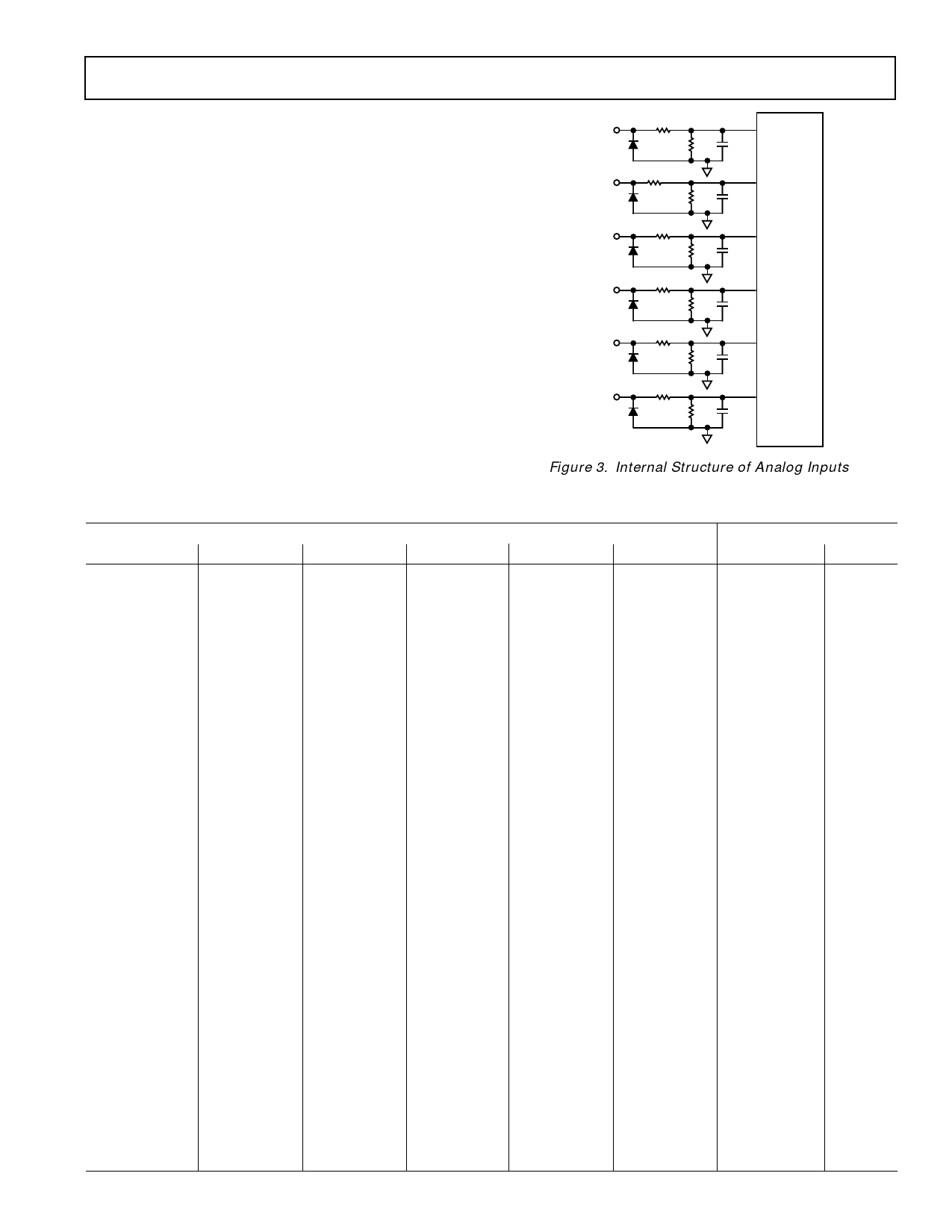
INPUT CIRCUITS
The internal structure for the analog inputs is shown in Figure
3. Each input circuit consists of an input protection diode, an
attenuator, plus a capacitor to form a first order low-pass filter
which gives the input immunity to high frequency noise.
+VCCP2
+12V
+5V
+3.3V
+2.5V
+VCCP1
42.7k⍀
97.3k⍀
122.2k⍀
22.7k⍀
91.6k⍀
55.2k⍀
61.1k⍀
80.9k⍀
36.7k⍀
111.2k⍀
42.7k⍀
97.3k⍀
ADM9240
50pF
35pF
25pF
MUX
25pF
25pF
50pF
Figure 3. Internal Structure of Analog Inputs
+12 VIN
<0.062
0.062–0.125
0.125–0.187
0.188–0.250
0.250–0.313
0.313–0.375
0.375–0.438
0.438–0.500
0.500–0.563
4.000–4.063
8.000–8.063
12.000–12.063
15.313–15.375
15.375–15.438
15.438–15.500
15.500–15.563
15.563–15.625
15.625–15.688
15.688–15.750
15.750–15.813
15.813–15.875
15.875–15.938
>15.938
REV. 0
+5 VIN
<0.026
0.026–0.052
0.052–0.078
0.078–0.104
0.104–0.130
0.130–0.156
0.156–0.182
0.182–0.208
0.208–0.234
1.666–1.692
3.330–3.560
5.000–5.026
6.380–6.406
6.406–6.432
6.432–6.458
6.458–6.484
6.484–6.510
6.510–6.536
6.536–6.562
6.562–6.588
6.588–6.615
6.615–6.640
>6.640
Table I. A/D Output Code vs. VIN
Input Voltage
+3.3 VIN
+2.5 VIN
<0.0172
0.017–0.034
0.034–0.052
0.052–0.069
0.069–0.086
0.086–0.103
0.103–0.120
0.120–0.138
0.138–0.155
1.100–1.117
2.200–2.217
3.300–3.317
4.210–4.230
4.230–4.245
4.245–4.263
4.263–4.280
4.280–4.300
4.300–4.314
4.314–4.331
4.331–4.348
4.348–4.366
4.366–4.383
>4.383
<0.013
0.013–0.026
0.026–0.039
0.039–0.052
0.052–0.065
0.065–0.078
0.078–0.091
0.091–0.104
0.104–0.117
l
l
l
0.833–0.846
l
l
l
1.667–1.680
l
l
l
2.500–2.513
l
l
l
3.190–3.203
3.203–3.216
3.216–3.229
3.229–3.242
3.242–3.255
3.255–3.268
3.268–3.281
3.281–3.294
3.294–3.307
3.307–3.320
>3.320
+VCCP1
<0.014
0.014–0.028
0.028–0.042
0.042–0.056
0.056–0.070
0.070–0.084
0.084–0.098
0.098–0.112
0.112–0.126
0.900–0.914
1.800–1.814
2.700–2.714
3.445–3.459
3.459–3.473
3.473–3.487
3.487–3.501
3.501–3.515
3.515–3.529
3.529–3.543
3.543–3.558
3.558–3.572
3.572–3.586
>3.586
+VCCP2
<0.014
0.014–0.028
0.028–0.042
0.042–0.056
0.056–0.070
0.070–0.084
0.084–0.098
0.098–0.112
0.112–0.126
0.900–0.914
1.800–1.814
2.700–2.714
3.445–3.459
3.459–3.473
3.473–3.487
3.487–3.501
3.501–3.515
3.515–3.529
3.529–3.543
3.543–3.558
3.558–3.572
3.572–3.586
>3.586
–9–
A/D Output
Decimal
Binary
0
00000000
1
00000001
2
00000010
3
00000011
4
00000100
5
00000101
6
00000110
7
00000111
8
00001000
64 (1/4 Scale) 01000000
128 (1/2 Scale) 10000000
192 (3/4 Scale) 11000000
245
11110101
246
11110110
247
11110111
248
11111000
249
11111001
250
11111010
251
11111011
252
11111100
253
11111101
254
11111110
255
11111111
Share Link: 