UAA3535HL データシートの表示(PDF) - Philips Electronics
部品番号
コンポーネント説明
メーカー
UAA3535HL Datasheet PDF : 24 Pages
| |||
Philips Semiconductors
Low power GSM/DCS/PCS multi-band transceiver
Objective specification
UAA3535HL
Transmit modulation loop
The analog transmit modulation loop consists of an
on-chip offset mixer, a phase-frequency detector, an
off-chip loop filter and a transmit VCO. The analog PLL
copies the modulation to the off-chip transmit VCO and
acts as a tracking filter. A PLL of at least third-order is
required to meet noise requirements at 20 MHz offset from
the carrier. The PLL bandwidth must be greater than
600 kHz in order to keep a low dynamic phase error and to
minimize the acquisition time.
RF and IF LO sections
The RF LO input covering the 1788 to 2002 MHz
bandwidth is connected to an external RF VCO module.
The RF LO section includes the LO buffering for the
RF PLL, a divider-by-2 or 1 for GSM and DCS/PCS
respectively which drives a quadrature generation network
for use in the RX I/Q down-mixer or the transmit
modulation loop offset mixer. The IF LO section consists of
a fully integrated IF VCO which internally provides the
I/Q modulator with the necessary quadrature signals.
Dual PLL
A high performance dual PLL is included on-chip which
enables the frequencies of the RF VCO to be synthesized
off-chip and that of the IF VCO on-chip. Very low close-in
phase noise is achieved which allows the PLL loop
bandwidth to be widened to achieve a shorter settling time.
The charge pump circuit has very low leakage current, in
the nA range, so that the spurious signals are hardly
detectable.
The ‘main’ path consists of a programmable divider chain
that divides the RF and IF LO signals down to frequencies
of 200 kHz (100 kHz step programmability) and 13 MHz
respectively. Their phase is then compared in a digital
Phase-Frequency Detector (PFD) with that of a reference
signal derived from an external 13 or 26 MHz clock signal.
The phase error information is fed back to the VCO via the
charge pump circuit that ‘sinks’ into or ‘sources’ current
from the loop filter capacitor, thereby changing the VCO
frequency so that the loop becomes ‘phase locked’.
Operating modes
BASIC OPERATING MODES
The circuit can be powered-up into different operating
modes depending on the voltage level applied at pins
RXON, TXON and SYNON (hardware control). This
defines the three main modes; RX, TX and SYN. Table 1
describes the different operating modes as defined by
hardware control.
The operation mode status depends on the control bits
SYNON, RXON and TXON (see Table 1).
When the receiver is on, it is possible to switch-off the low
noise amplifier to perform DC offset compensation in the
receiver (see Section “LNA power control”).
When in TX mode, it is possible to enable the
IF synthesizer and VCO independently from the rest of the
TX section via bit TXIFON via the control bus.
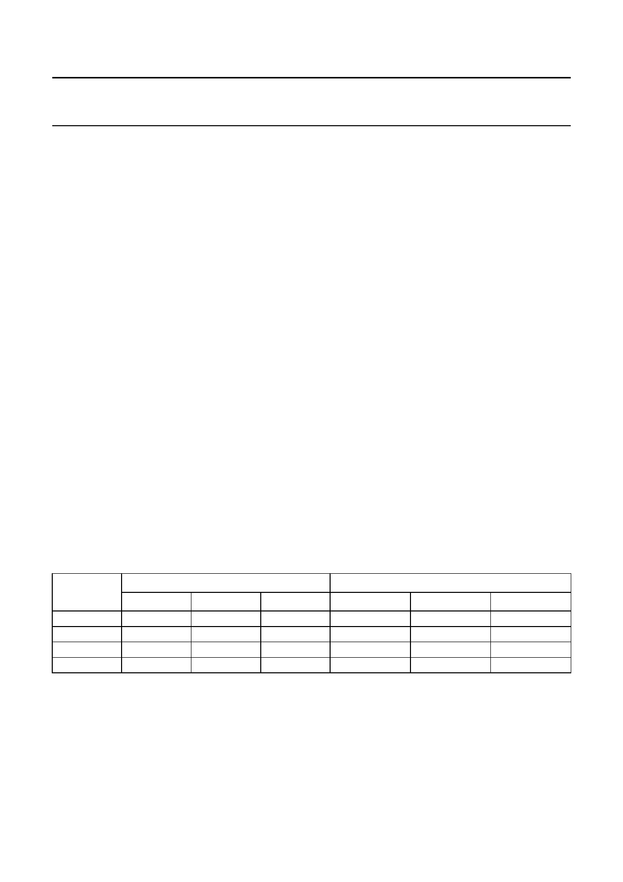
Table 1 Basic operating mode control
MODE
SYN
RX
TX
Idle
CONTROL PIN LEVEL
SYNON
RXON
TXON
HIGH
HIGH
HIGH
LOW
LOW
HIGH
LOW
LOW
LOW
LOW
HIGH
LOW
POWER STATUS
SYNTHESIZER RECEIVER TRANSMITTER
on
off
off
on
on
off
on
off
on
off
off
off
2000 Feb 17
6
Share Link: 