UCLAMP3301D.TCT гГЗгГЉгВњгВЈгГЉгГИгБЃи°®з§ЇпЉИPDFпЉЙ - Semtech Corporation
йГ®еУБзХ™еПЈ
гВ≥гГ≥гГЭгГЉгГНгГ≥гГИи™ђжШО
гГ°гГЉгВЂгГЉ
UCLAMP3301D.TCT Datasheet PDF : 6 Pages
| |||
uClamp3301D
PROTECTION PRODUCTS
Applications Information
Device Connection Options
The µClamp3301D is designed to protect one I/O, or
power supply line. It will present a high impedance to
the protected line up to 3.3 volts. It will вАЬturn onвАЭ
when the line voltage exceeds 3.5 volts. The device is
unidirectional and may be used on lines where the
signal polarity is above ground. The cathode band
should be placed towards the line that is to be
protected.
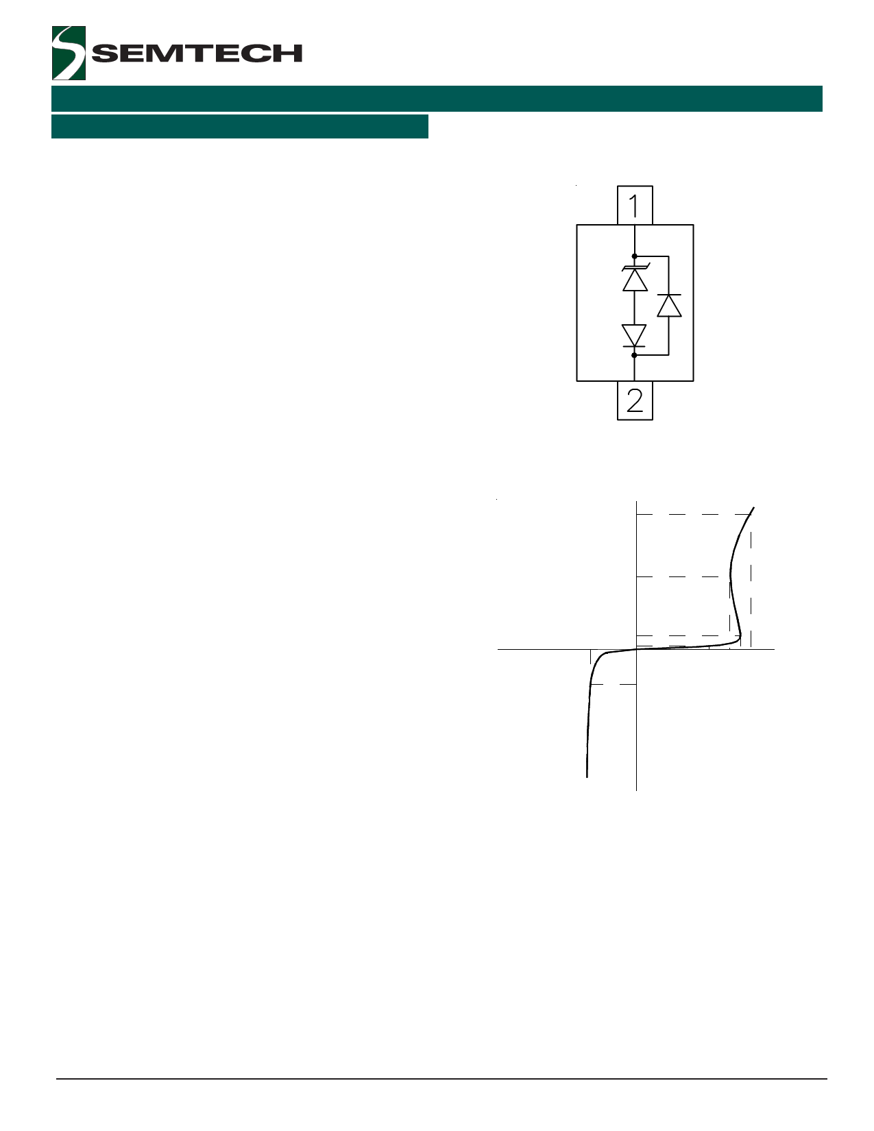
Device Schematic & Pin Configuration
Due to the вАЬsnap-backвАЭ characteristics of the low
voltage TVS, it is not recommended that the I/O line be
directly connected to a DC source greater than snap-
back votlage (VSB) as the device can latch on as
described below.
EPD TVS Characteristics
The ¬µClamp3301D is constructed using SemtechвАЩs
proprietary EPD technology. The structure of the EPD
TVS is vastly different from the traditional pn-junction
devices. At voltages below 5V, high leakage current
and junction capacitance render conventional ava-
lanche technology impractical for most applications.
However, by utilizing the EPD technology, the
µClamp3301D can effectively operate at 3.3V while
maintaining excellent electrical characteristics.
The EPD TVS employs a complex nppn structure in
contrast to the pn structure normally found in tradi-
tional silicon-avalanche TVS diodes. Since the EPD
TVS devices use a 4-layer structure, they exhibit a
slightly different IV characteristic curve when compared
to conventional devices. During normal operation, the
device represents a high-impedance to the circuit up to
the device working voltage (VRWM). During an ESD
event, the device will begin to conduct and will enter a
low impedance state when the punch through voltage
(VPT) is exceeded. Unlike a conventional device, the low
voltage TVS will exhibit a slight negative resistance
characteristic as it conducts current. This characteris-
tic aids in lowering the clamping voltage of the device,
but must be considered in applications where DC
voltages are present.
When the TVS is conducting current, it will exhibit a
slight вАЬsnap-backвАЭ or negative resistance characteris-
tics due to its structures. This point is defined on the
curve by the snap-back voltage (VSB) and snap-back
EPD TVS IV Characteristic Curve
IPP
ISB
IPT
VF
IR
IF
VRWM VSB VPT VC
current (ISB). To return to a non-conducting state, the
current through the device must fall below the ISB
(approximately <50mA) and the voltage must fall below
the VSB (normally 2.8 volts for a 3.3V device). If a 3.3V
TVS is connected to 3.3V DC source, it will never fall
below the snap-back voltage of 2.8V and will therefore
stay in a conducting state.
п£© 2008 Semtech Corp.
4
www.semtech.com
Share Link: 