A67L7332E-5 データシートの表示(PDF) - AMIC Technology
部品番号
コンポーネント説明
メーカー
A67L7332E-5 Datasheet PDF : 19 Pages
| |||
A67L8316/A67L8318/
A67L7332/A67L7336 Series
Pin Description
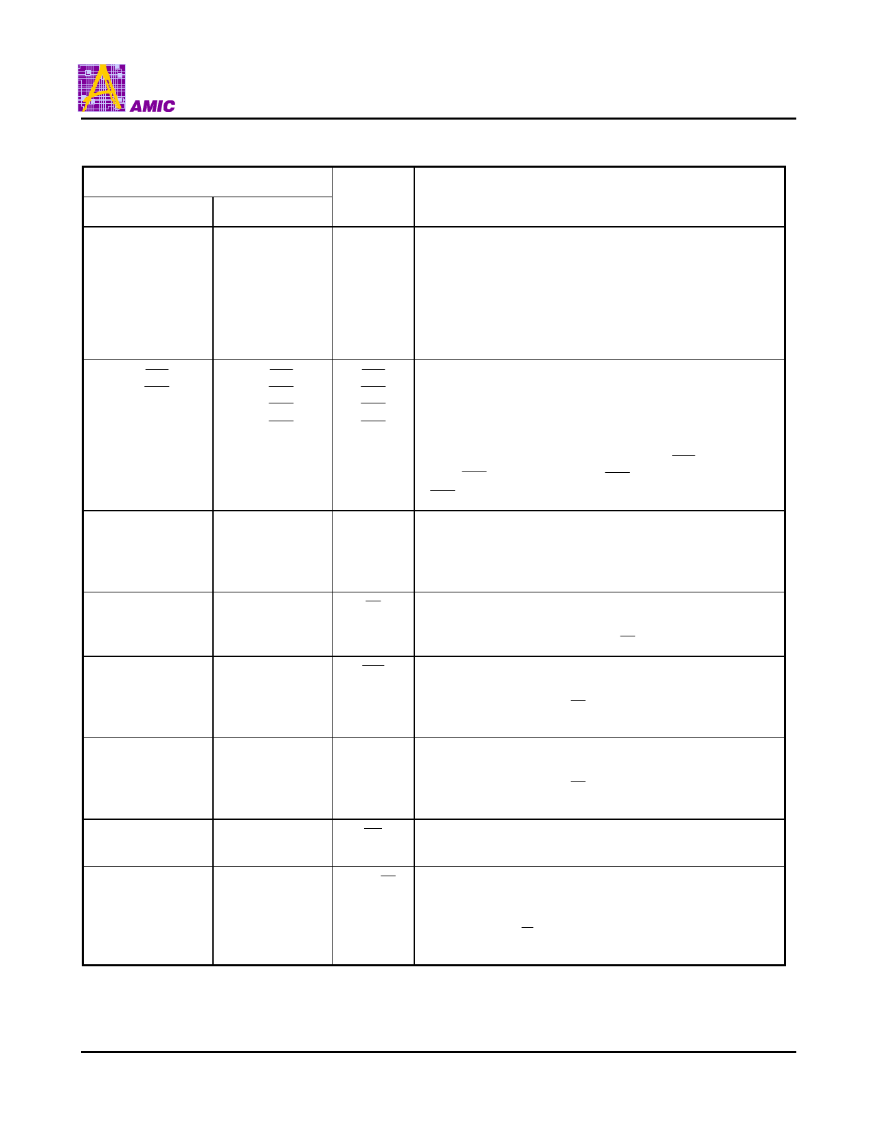
Pin No.
LQFP (X16/X18) LQFP (X32/X36)
37
36
35,34,33,32,
100,99,82,81,
44,45,46,47,
48,49,50
80
37
36
35,34,33,32,
100,99,82,81,
44,45,46,47,
48,49,50
93 (BW1)
94 (BW2 )
93 (BW1)
94 (BW2 )
95 (BW3 )
96 (BW4 )
Symbol
A0
A1
A2 - A16
A17
BW1
BW2
BW3
BW4
89
89
CLK
98
98
CE
92
92
CE2
97
97
CE2
86
86
OE
85
85
ADV/ LD
Description
Synchronous Address Inputs : These inputs are registered
and must meet the setup and hold times around the rising
edge of CLK. Pins 83 and 84 are reserved as address bits
for higher-density 9Mb and 18Mb DBA SRAMs, respectively.
A0 and A1 are the two lest significant bits (LSB) of the
address field and set the internal burst counter if burst is
desired.
Synchronous Byte Write Enables : These active low inputs
allow individual bytes to be written when a WRITE cycle is
active and must meet the setup and hold times around the
rising edge of CLK. BYTE WRITEs need to be asserted on
the same cycle as the address, BWs are associated with
addresses and apply to subsequent data. BW1 controls I/Oa
pins; BW2 controls I/Ob pins; BW3 controls I/Oc pins;
BW4 controls I/Od pins.
Clock: This signal registers the address, data, chip enables,
byte write enables and burst control inputs on its rising
edge. All synchronous inputs must meet setup and hold
times around the clock are rising edge.
Synchronous Chip Enable : This active low input is used to
enable the device. This input is sampled only when a new
external address is loaded (ADV/LD LOW).
Synchronous Chip Enable : This active low input is used to
enable the device and is sampled only when a new external
address is loaded (ADV/LD LOW). This input can be used
for memory depth expansion.
Synchronous Chip Enable : This active high input is used to
enable the device and is sampled only when a new external
address is loaded (ADV/LD LOW). This input can be used
for memory depth expansion.
Output Enable : This active low asynchronous input enables
the data I/O output drivers.
Synchronous Address Advance/Load : When HIGH, this
input is used to advance the internal burst counter,
controlling burst access after the external address is loaded.
When HIGH, R/ W is ignored. A LOW on this pin permits a
new address to be loaded at CLK rising edge.
PRELIMINARY (March, 1999, Version 0.0)
5
AMIC Technology, Inc.
Share Link: 