UPA1810 データシートの表示(PDF) - NEC => Renesas Technology
部品番号
コンポーネント説明
メーカー
UPA1810 Datasheet PDF : 8 Pages
| |||
ELECTRICAL CHARACTERISTICS (TA = 25 °C)
CHARACTERISTICS
SYMBOL
TEST CONDITIONS
Zero Gate Voltage Drain Current
IDSS
VDS = –12 V, VGS = 0 V
Gate Leakage Current
IGSS
VGS = ±10 V, VDS = 0 V
Gate Cut-off Voltage
VGS(off) VDS = –10 V, ID = –1 mA
Forward Transfer Admittance
| yfs | VDS = –10 V, ID = –2.0 A
Drain to Source On-state Resistance
RDS(on)1 VGS = –4.5 V, ID = –2.0 A
RDS(on)2 VGS = –4.0 V, ID = –2.0 A
RDS(on)3 VGS = –2.5 V, ID = –2.0 A
Input Capacitance
Ciss
VDS = –10 V
Output Capacitance
Coss
VGS = 0 V
Reverse Transfer Capacitance
Crss
f = 1 MHz
Turn-on Delay Time
td(on)
VDD = –10 V
Rise Time
tr
ID = –2.0 A
Turn-off Delay Time
td(off)
VGS(on) = –4.0 V
Fall Time
tf
RG = 5 Ω
Total Gate Charge
QG
VDD = –10 V
Gate to Source Charge
QGS ID = –4.0 A
Gate to Drain Charge
QGD VGS = –4.0 V
Diode Forward Voltage
VF(S-D) IF = 4.0 A, VGS = 0 V
Reverse Recovery Time
Reverse Recovery Charge
trr
IF = 4.0 A, VGS = 0 V
Qrr
di/dt = 100 A/µS
µ PA1810
MIN. TYP. MAX. UNIT
–10 µA
±10 µA
–0.5 –0.8 –1.5 V
2.5 8.5
S
41 55 mΩ
43 60 mΩ
71 100 mΩ
1100
pF
750
pF
240
pF
40
ns
100
ns
90
ns
70
ns
35
nC
5
nC
16
nC
0.75
V
50
ns
35
nC
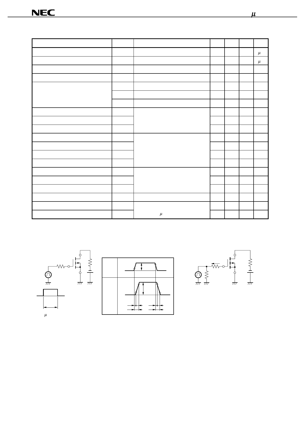
TEST CIRCUIT 1 SWITCHING TIME
D.U.T.
RG
PG.
RG = 10 Ω
VGS
0
τ
τ = 1µ s
Duty Cycle ≤ 1 %
RL
VDD
VGS
VGS
Wave Form
010 %
VGS(on)
ID
90 %
ID
Wave Form
0 10 %
td(on)
ID
tr td(off)
90 %
90 %
10 %
tf
ton
toff
TEST CIRCUIT 2 GATE CHARGE
D.U.T.
IG = 2 mA
RL
PG.
50 Ω
VDD
2
Data Sheet D11819EJ1V0DS00
Share Link: 