UPB1502GR-E2 データシートの表示(PDF) - NEC => Renesas Technology
部品番号
コンポーネント説明
メーカー
UPB1502GR-E2
NEC => Renesas Technology

UPB1502GR-E2 Datasheet PDF : 16 Pages
| |||
µPB1502GR, 1502GR(1)
PIN DESCRIPTIONS
Pin No. Symbol
Assignment
Functions and Explanation
1
IN
Frequency input pin Input frequency from an external VCO output.
Must be coupled with capacitor (e.g. 1 000 pF) for DC cut.
2
VCC
Power supply pin
Supply voltage 3.0 ± 0.3 V for operation. Must be connected bypass
capacitor (e.g. 1 000 pF) to minimize ground impedance.
3
SW
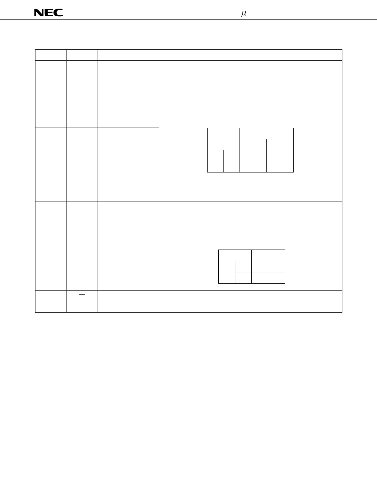
Divided ratio
Divided ratio and modulus control can be governed by following input
control input pin
data to these pins.
6
M
Modulus
control input pin
H
SW
L
M
H
L
1/64
1/65
1/128
1/129
4
OUT Divided frequency
This frequency output can be interfaced to CMOS PLL.
output pin
Must be coupled with capacitor (e.g. 1 000 pF) for DC cut.
5
GND Ground pin
Must be connected to the system ground with minimum inductance.
Ground pattern on the board should be formed as wide as possible.
(Track length should be kept as short as possible).
7
VPS
Power-save
function pin
ON/OFF-operation control can be governed by following input data to
this pin.
Operation
H
VPS
L
ON
OFF
8
IN
Frequency-input
Must be connected bypass capacitor (e.g. 1 000 pF) to minimize
bypass pin
ground impedance.
4
Data Sheet P10871EJ3V0DS00
Share Link: