UPB1009K-E1 データシートの表示(PDF) - NEC => Renesas Technology
部品番号
コンポーネント説明
メーカー
UPB1009K-E1
NEC => Renesas Technology

UPB1009K-E1 Datasheet PDF : 27 Pages
| |||
UPB1009K
PRODUCT LINE-UP (TA = +25°C, VCC = 3.0 V)
Type Part Number
Functions
(Frequency unit: MHz)
VCC
ICC
(V)
(mA)
Clock
Frequency
Specific
1 chip IC
µPB1009K
Pre-amplifier + RF/IF down- 2.7 to 3.3 26.0
converter + PLL synthesizer
REF = 16.368
1stIF = 61.380/2ndIF = 4.092
REF = 14.4, 16.384, 19.2, 26
1stIF = 62.980/2ndIF = 2.556
On-chip 4-bit ADC
µPB1008K
LNA + Pre-amplifier + RF/IF 2.7 to 3.3 18.0
down-converter + PLL
synthesizer
REF = 27.456
1stIF = 175.164/2ndIF = 0.132
On-chip 2-bit ADC
µPB1007K
Pre-amplifier + RF/IF down- 2.7 to 3.3 25.0
converter + PLL synthesizer
REF = 16.368
1stIF = 61.380/2ndIF = 4.092
µPB1005K
REF = 16.368
1stIF = 61.380/2ndIF = 4.092
CG
Package
(dB)
44-pin plastic QFN
100 to 36-pin plastic QFN
120
100 to 36-pin plastic QFN
120
36-pin plastic QFN
Status
New Device
Available
Remark Typical performance. Please refer to ELECTRICAL CHARACTERISTICS in detail.
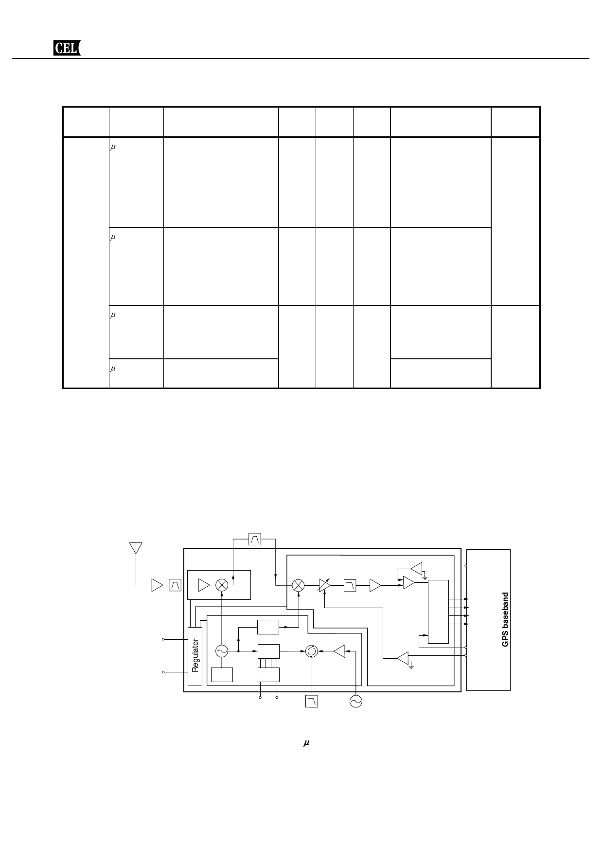
SYSTEM APPLICATION EXAMPLE
GPS receiver RF block diagram
PD1 and PD2 in the figure are Power Save Mode control pins.
MS1 and MS2 in the figure are TXCO (GPS, W-CDMA, PDC, GSM) control pins.
RF =
1575.42 MHz
1stIF =
61.38 MHz
1stLo =
62.98 MHz
1636.8 MHz
1638.4 MHz
IF SAW
2ndIF =
4.092 MHz
2.556 MHz
RF
LNA SAW
Pre- 1st.
amp mix
RF
2nd
IF
MIX AGC LPF Amp
–
+
+
–
PD1
PD2
Tank
÷25
÷N
Cont.
IF
PLL
4bit
ADC
–
+
DC trim
Para Data
Samp Clk
AGC cont
MS1 MS2
TCXO
Caution This diagram schematically shows only the µPB1009K’s internal functions on the system.
This diagram does not present the actual application circuits.
3
Share Link: