UPB1009K-E1 データシートの表示(PDF) - NEC => Renesas Technology
部品番号
コンポーネント説明
メーカー
UPB1009K-E1
NEC => Renesas Technology

UPB1009K-E1 Datasheet PDF : 27 Pages
| |||
UPB1009K
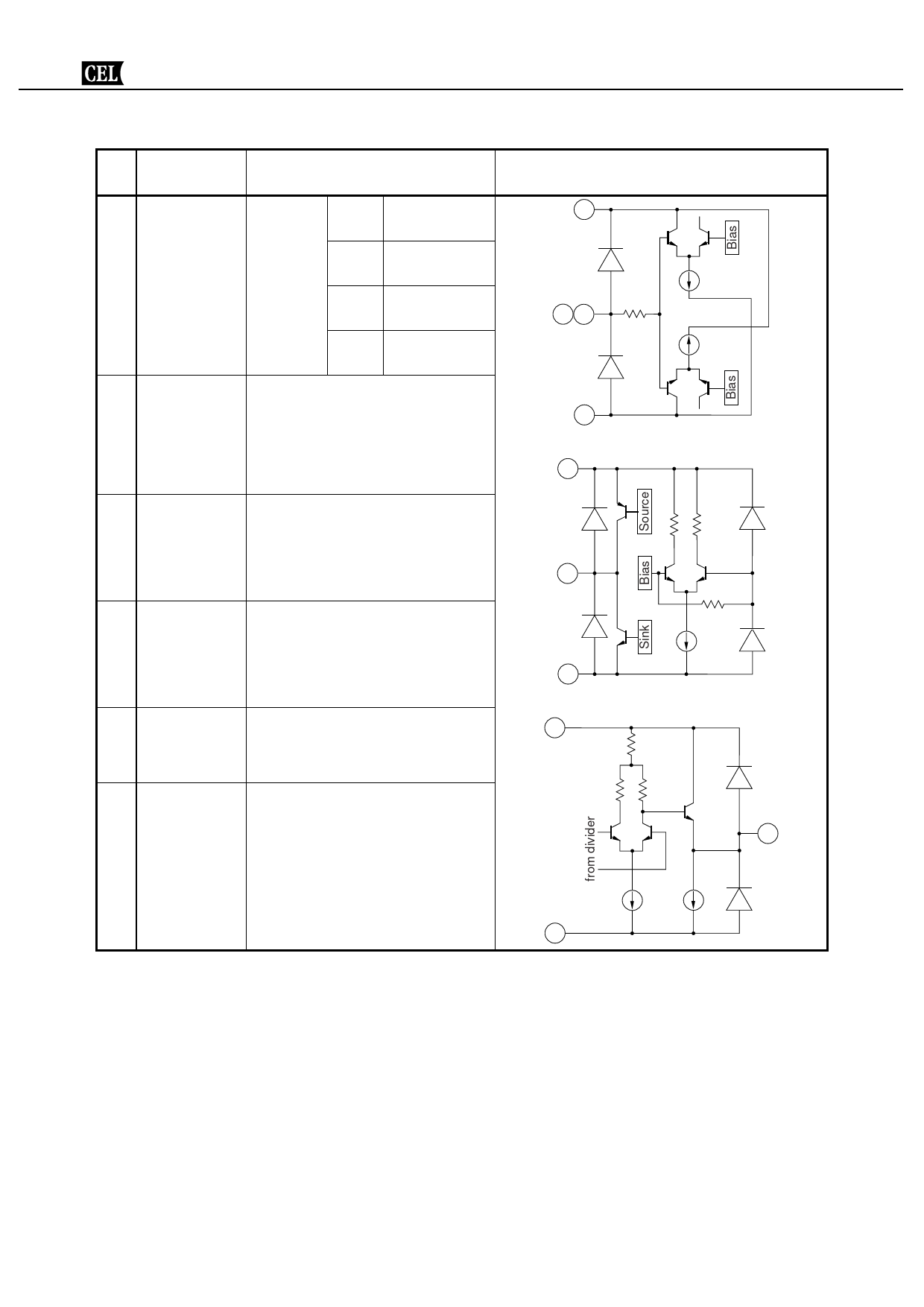
Pin
Pin Name
No.
6 MS1
12 MS2
11 CPout
Function and Application
Low :
MS1 : L TCXO : 16.368,
0 to 0.3 (V) MS2 : L 16.384 MHz
High :
MS1 : L TCXO : 19.2 MHz
VCC − 0.3 to MS2 : H
VCC (V)
MS1 : H TCXO : 14.4 MHz
MS2 : L
MS1 : H TCXO : 26 MHz
MS2 : H
Output pin of charge pump. Connect
external R and C to this pin to set a
dumping factor and natural angular
frequency (Isink = Isource = 0.45 mA).
13 Refin
Reference frequency input pin. Connect
an external reference transmitter (such as
TCXO) to this pin.
14 PLLVCC
Power supply voltage pin of PLL.
Connect a bypass capacitor to this pin to
reduce the high-frequency impedance.
15 PLLGND
Ground pin of PLL.
16 CLKout
Clock (fTCXO) output pin (IC test pin).
Internal Equivalent Circuit
14
12 6
15
14
11
15
14
16
15
6
Share Link: