UPB1007K データシートの表示(PDF) - California Eastern Laboratories.
部品番号
コンポーネント説明
メーカー
UPB1007K Datasheet PDF : 9 Pages
| |||
UPB1007K
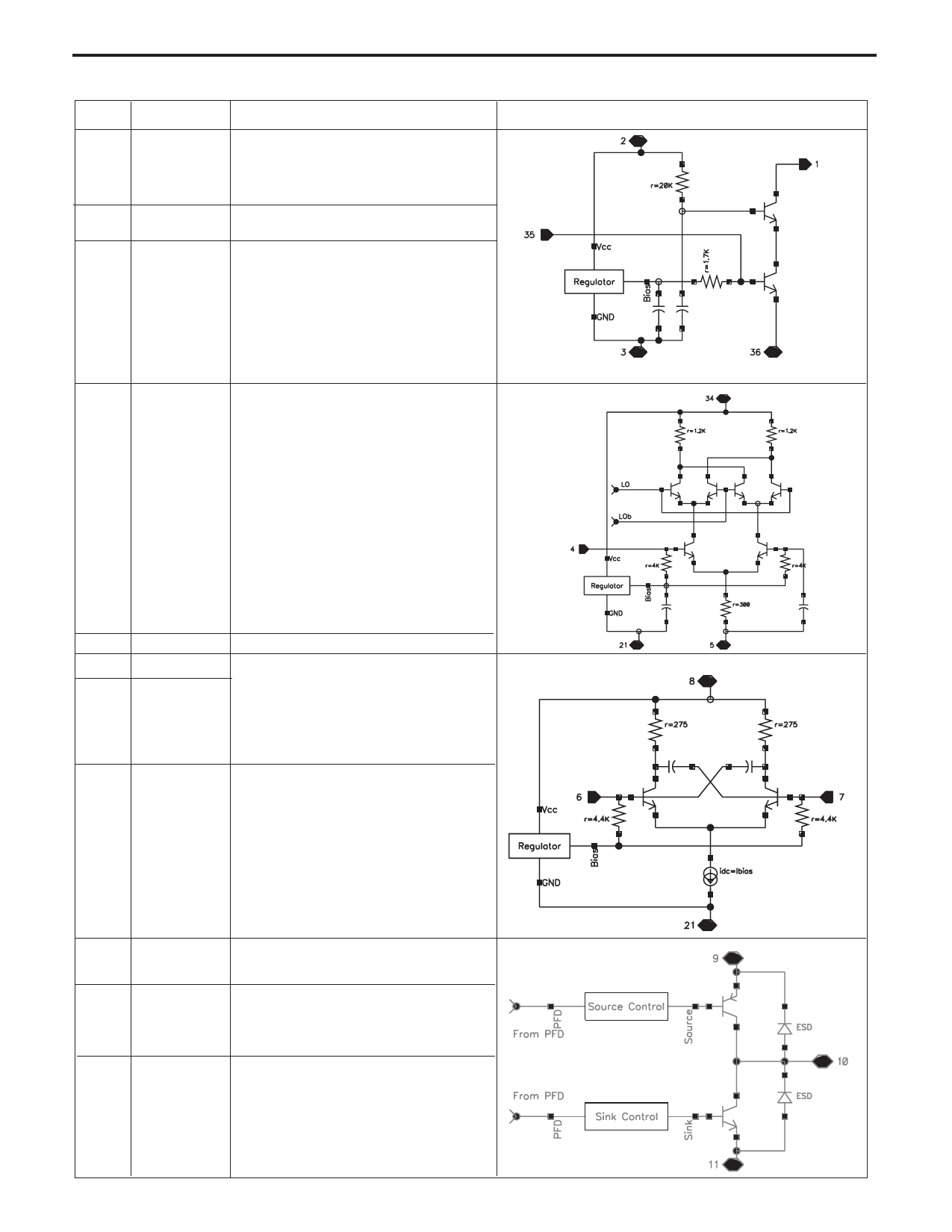
PIN FUNCTIONS
Pin No.
Symbol
Function and Application
1
LNAout
Output pin of LNA. Output biasing
and matching required as it is an open
collector output.
2
VCC (Vreg)
Supply voltage pin of regulator mixer
block.
3
GND (Vreg)
Ground pin of regulator reference cell.
4
RF MIXin
Input pin of RF mixer. 1575.42 MHz
band pass filter can be inserted between
pin 1 and mixer input.
Internal Equivalent Circuit
5
GND (MIX)
Ground pin of RF mixer cell.
6
1stLO-OSC1
Pins 6 & 7 are base pins of the differential
amplifier for 1st LO oscillator. These pins
7
1stLO-OSC2
should be equipped with LC and varactor
circuits to oscillate at 1636.8 MHz.
Supply voltage pin of differential amplifier
8 VCC (1stLO-OSC) for 1st LO oscillator circuit (VCO).
9
VCC
Supply voltage pin of the phase detector
(Charge Pump) charge pump.
10
PD-out
This is a current mode charge pump
output for connection to a passive RC
loop filter for driving the external varactor
diode of 1stLO-OSC.
11
GND
Ground pin of phase detector charge
(Charge Pump) pump.
Share Link: 