UPD120NXX データシートの表示(PDF) - NEC => Renesas Technology
部品番号
コンポーネント説明
メーカー
UPD120NXX
NEC => Renesas Technology

UPD120NXX Datasheet PDF : 15 Pages
| |||
µPD120Nxx Series
ABSOLUTE MAXIMUM RATINGS (TA = 25°C, unless otherwise specified.)
Parameter
Symbol
Rating
µ PD120NxxTA
µ PD120NxxT1B
Input Voltage
Power Dissipation Note1
VIN
−0.3 to +6
PT
180/510 Note2
400/2000 Note3
Operating Ambient Temperature
TA
–40 to +85
Operating Junction Temperature
TJ
–40 to +150
Storage Temperature
Thermal Resistance (junction to ambient)
Tstg
Rth(J-A)
–55 to +150
695/245 Note2
315/62.5 Note3
Unit
V
mW
°C
°C
°C
°C/W
Note 1. Internally limited. When the operating junction temperature rises over 150°C, the internal circuit shuts down
the output voltage.
2. Mounted on ceramic substrate of 75 mm2 x 0.7 mm
3. Mounted on ceramic substrate of 16 cm2 x 0.7 mm
Caution Product quality may suffer if the absolute maximum rating is exceeded even momentarily for any
parameter. That is, the absolute maximum ratings are rated values at which the product is on the
verge of suffering physical damage, and therefore the product must be used under conditions that
ensure that the absolute maximum ratings are not exceeded.
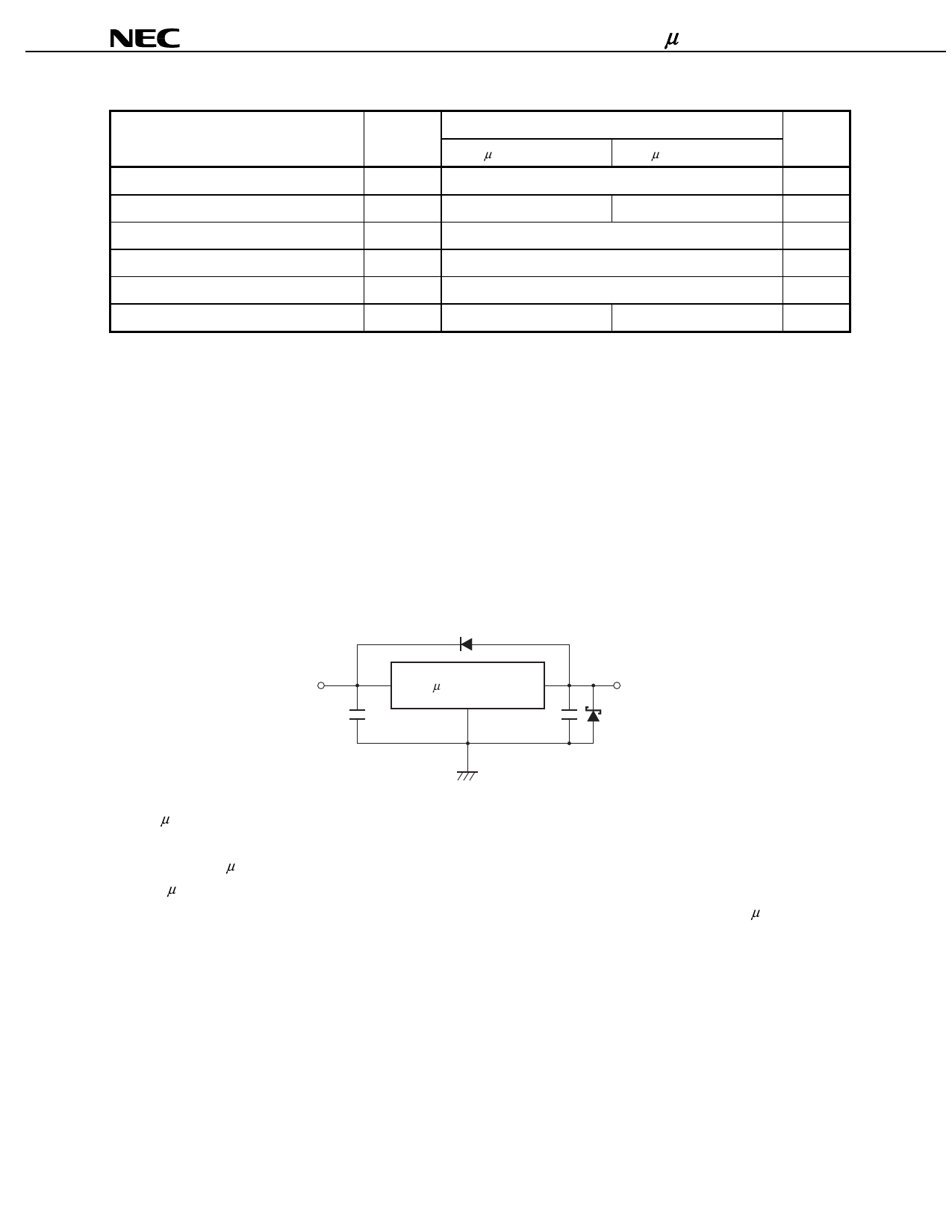
STANDARD CONNECTION
D1
INPUT
CIN
µ PD120Nxx
COUT
OUTPUT
D2
CIN: 0.1 µF or higher. Set this value according to the length of the line between the regulator and INPUT pin. Be sure
to connect CIN to prevent parasitic oscillation. If using a laminated ceramic capacitor, it is necessary to ensure
that CIN is 0.1 µF or higher for the voltage and temperature range to be used.
COUT: 10 µF or higher. Be sure to connect COUT to prevent oscillation and improve excessive load regulation. Place
CIN and COUT as close as possible to the IC pins (within 2 cm). Be sure to use the capacitor of 10 µF or higher
of capacity values and 1 to 8 Ω of equivalent series resistance under an operating condition.
D1: If the OUTPUT pin has a higher voltage than the INPUT pin, connect a diode.
D2: If the OUTPUT pin has a lower voltage than the GND pin, connect a schottky barrier diode.
Caution Make sure that no voltage is applied to the OUTPUT pin from external.
4
Data Sheet S17145EJ2V0DS
Share Link: