UPD16705N-XXX データシートの表示(PDF) - NEC => Renesas Technology
部品番号
コンポーネント説明
メーカー
UPD16705N-XXX Datasheet PDF : 12 Pages
| |||
µPD16705
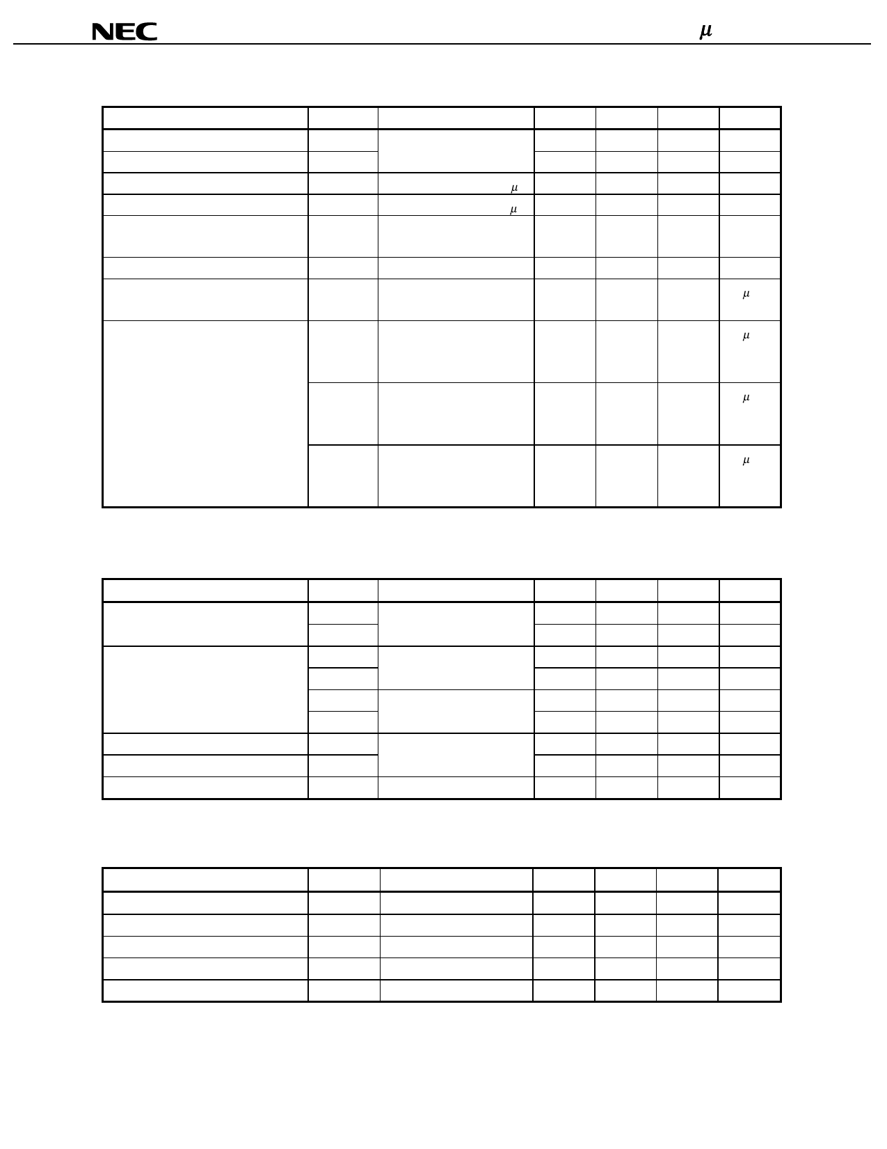
Electrical Characteristics (TA = −20 to +75°C, VDD1 = 2.3 to 3.6 V, VDD2 = 23 V, VEE = −10 V, VSS = 0 V)
Parameter
Symbol
Condition
MIN.
TYP.Note
MAX.
Unit
High-level Input Voltage
Low-level Input Voltage
High-level Output Voltage
Low-level Output Voltage
VIH
CLK, STVR (STVL), R,/L,
0.8 VDD1
VIL
OE1 to OE3
VSS
VOH
STVR (STVL), IOH = −40 µA VDD1 −0.4
VOL
STVR (STVL), IOL = +40 µA
VSS
VDD1
V
0.2 VDD1
V
VDD1
V
VSS +0.4
V
LCD Driver Output ON Resistance RON
VOUT = VEE +1.0 V, or
VDD2 −1.0 V
0.33
1.0
kΩ
Pull-up Resistance
Input Leak Current
RPU
VDD1 = 3.3 V, /AO, MODE
10
50
100
kΩ
IIL
VI = 0 V or 3.6 V,
±1.0
µA
except for /AO, MODE
Static Current Dissipation
IDD1
VDD1, fCLK = 50 kHz,
OE1 = OE2 = OE3 = L,
fSTV = 60 Hz, no load
390
1000
µA
IDD2
VDD2, fCLK = 50 kHz,
OE1 = OE2 = OE3 = L,
fSTV = 60 Hz, no load
10
100
µA
IEE
VEE, fCLK = 50 kHz,
−1100
−400
µA
OE1 = OE2 = OE3 = L,
fSTV = 60 Hz, no load
Remark STV: STVR (STVL).
Switching Characteristics (TA = −20 to +75°C, VDD1 = 2.3 to 3.6 V, VDD2 = 23 V, VEE = −10 V, VSS = 0 V)
Parameter
Symbol
Condition
MIN.
TYP.
MAX.
Unit
Cascade Output Delay Time
Driver Output Delay Time
Output Rise Time
Output Fall Time
Input Capacitance
tPHL1
tPLH1
tPHL2
tPLH2
tPHL3
tPLH3
tTLH
tTHL
CI
CL = 20 pF,
CLK → STVL (STVR)
CL = 300 pF, CLK → On
CL = 300 pF, OEn → On
CL = 300 pF
TA = 25°C
800
ns
800
ns
500
ns
500
ns
800
ns
800
ns
800
ns
800
ns
15
pF
Timing Requirements (TA = −20 to +75°C, VDD1 = 2.3 to 3.6 V, VDD2 = 23 V, VEE = −10 V, VSS = 0 V,
tr = tf = 20 ns (10 to 90%))
Parameter
Symbol
Condition
MIN.
TYP.
MAX.
Unit
Clock Pulse High Width
PWCLK(H)
500
ns
Clock Pulse Low Width
PWCLK(L)
500
ns
Enable Pulse Width
PWOE
1000
ns
Data Setup Time
tSETUP
STVR (STVL) ↑ → CLK ↑
200
ns
Data Hold Time
tHOLD
CLK ↑ → STVR (STVL) ↓
200
ns
Remark Unless otherwise specified, the input level is defined to be VIH = 0.8 VDD1, VIL = 0.2 VDD1.
8
Data Sheet S15818EJ1V0DS
Share Link: 